AO3415
Description
The AO3415 uses advanced trench technology to provide excellent RDS(ON), low gate charge and operation with gate voltages as low as 1.8V. This device is suitable for use as a load switch applications.
Product Summary
VDS ID (at VGS=-4.5V) RDS(ON) (at VGS= -4.5V) RDS(ON) (at VGS= -2.5V) RDS(ON) (at VGS= -1.8V) ESD protected -20V -4A < 41mΩ < 53mΩ < 65mΩ
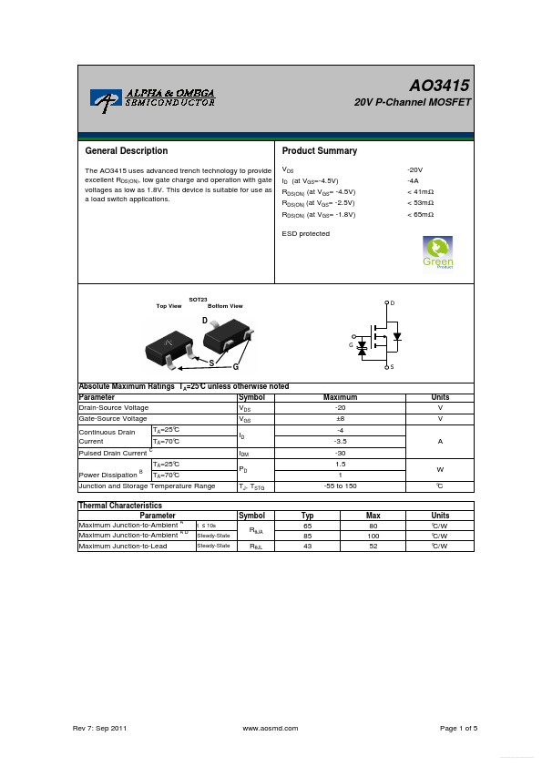
SOT23 Top View Bottom View
Absolute Maximum Ratings TA=25° C unless otherwise noted Parameter Symbol Drain-Source Voltage VDS Gate-Source Voltage Continuous Drain Current Pulsed Drain Current Power Dissipation B
Maximum -20 ±8 -4 -3.5 -30 1.5 1 -55 to 150
Units V V A
VGS TA=25° C TA=70° C TA=25° C TA=70° C ID IDM PD TJ, TSTG
W ° C
Junction and Storage Temperature Range Thermal Characteristics Parameter Maximum Junction-to-Ambient A Maximum Junction-to-Ambient A D Maximum Junction-to-Lead
Symbol t ≤ 10s Steady-State Steady-State
RθJA RθJL
Typ 65 85 43
Max 80 100 52
Units ° C/W ° C/W ° C/W
Rev...