The following content is an automatically extracted verbatim text
from the original manufacturer datasheet and is provided for reference purposes only.
View original datasheet text
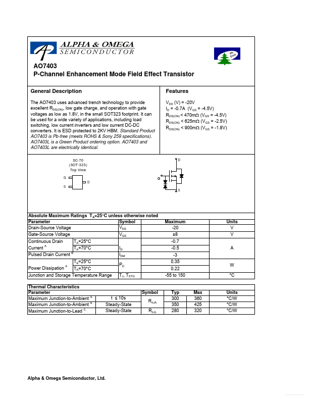
AO7403 P-Channel Enhancement Mode Field Effect Transistor
General Description
The AO7403 uses advanced trench technology to provide excellent RDS(ON), low gate charge, and operation with gate voltages as low as 1.8V, in the small SOT323 footprint. It can be used for a wide variety of applications, including load switching, low current inverters and low current DC-DC converters. It is ESD protected to 2KV HBM. Standard Product AO7403 is Pb-free (meets ROHS & Sony 259 specifications). AO7403L is a Green Product ordering option. AO7403 and AO7403L are electrically identical.
SC-70 (SOT-323) Top View G D S G S
Features
VDS (V) = -20V ID = -0.7A (VGS = -4.5V) RDS(ON) < 470mΩ (VGS = -4.5V) RDS(ON) < 625mΩ (VGS = -2.5V) RDS(ON) < 900mΩ (VGS = -1.
 AO7403 Datasheet