Datasheet Details
| Part number | AON6442 |
|---|---|
| Manufacturer | Alpha & Omega Semiconductors |
| File Size | 478.65 KB |
| Description | 40V N-Channel MOSFET |
| Download | AON6442 Download (PDF) |
|
|
Overview: AON6442 40V N-Channel MOSFET General.
| Part number | AON6442 |
|---|---|
| Manufacturer | Alpha & Omega Semiconductors |
| File Size | 478.65 KB |
| Description | 40V N-Channel MOSFET |
| Download | AON6442 Download (PDF) |
|
|
|
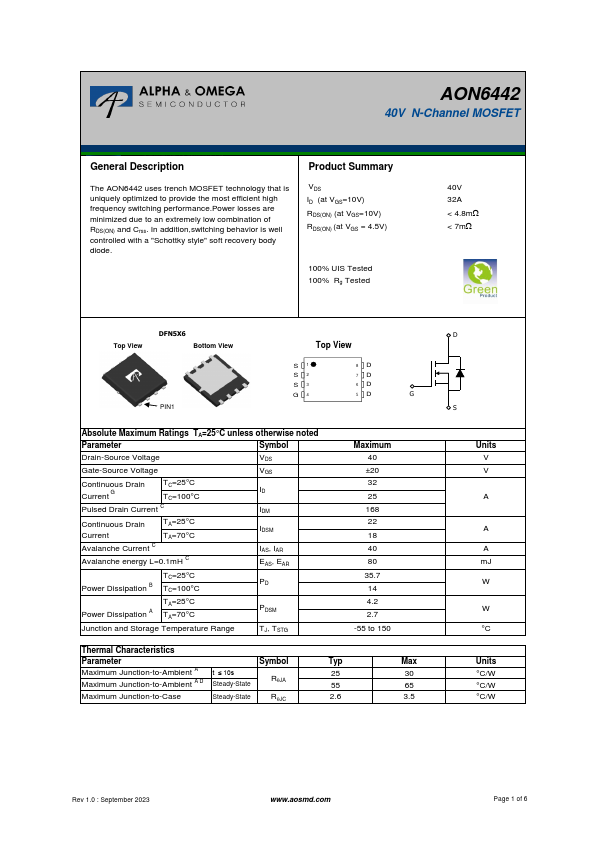
The AON6442 uses trench MOSFET technology that is uniquely optimized to provide the most efficient high frequency switching performance.Power losses are minimized due to an extremely low combination of RDS(ON) and Crss.
In addition,switching behavior is well controlled with a "Schottky style" soft recovery body diode.
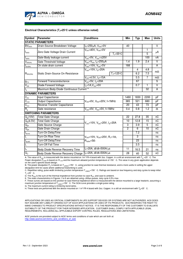
Product Summary VDS ID (at VGS=10V) RDS(ON) (at VGS=10V) RDS(ON) (at VGS = 4.5V) 100% UIS Tested 100% Rg Tested 40V 32A < 4.8mW < 7mW Top View DFN5X6 Bottom View PIN1 Top View S1 S2 S3 G4 8D 7D 6D 5D G Absolute Maximum Ratings TA=25°C unless otherwise noted Parameter Symbol Drain-Source Voltage VDS Gate-Source Voltage Continuous Drain TC=25°C Current G TC=100°C Pulsed Drain Current C Continuous Drain Current Avalanche Current C TA=25°C TA=70°C Avalanche energy L=0.1mH C VGS ID IDM IDSM IAS, IAR EAS, EAR TC=25°C Power Dissipation B TC=100°C PD TA=25°C Power Dissipation A TA=70°C PDSM Junction and Storage Temperature Range TJ, TSTG Maximum 40 ±20 32 25 168 22 18 40 80 35.7 14 4.2 2.7 -55 to 150 Thermal Characteristics Parameter Symbol Typ Maximum Junction-to-Ambient A t ≤ 10s Maximum Junction-to-Ambient A D Steady-State RqJA 25 55 Maximum Junction-to-Case Steady-State RqJC 2.6 Max 30 65 3.5 D S Units V V A A A mJ W W °C Units °C/W °C/W °C/W Rev 1.0 : September 2023 www.aosmd.com Page 1 of 6 AON6442 Electrical Characteristics (TJ=25°C unless otherwise noted) Symbol Parameter Conditions Min Typ Max Units STATIC PARAMETERS BVDSS Drain-Source Breakdown Voltage ID=250mA, VGS=0V 40 V IDSS Zero Gate Voltage Drain Current VDS=40V, VGS=0V TJ=55°C 1 5 mA IGSS Gate-Body leakage current VDS=0V, VGS=±20V 100 nA VGS(th) Gate Threshold Voltage VDS=VGS ID=250mA 1.4 1.9 2.4 V ID(ON) On state drain current VGS=10V, VDS=5V 168 A RDS(ON) Static Drain-Source On-Resistance VGS=10V, ID=20A TJ=125°C 4 4.8 6.2 7.5 mW VGS=4.5V, ID=15A 5.5 7
| Part Number | Description |
|---|---|
| AON6440 | N-Channel MOSFET |
| AON6444 | N-Channel MOSFET |
| AON6448 | N-Channel MOSFET |
| AON6400 | N-Channel MOSFET |
| AON6403 | 30V P-Channel MOSFET |
| AON6403L | N-Channel MOSFET |
| AON6404 | N-Channel MOSFET |
| AON6404A | N-Channel MOSFET |
| AON6404L | N-Channel MOSFET |
| AON6405 | 30V P-Channel MOSFET |