Datasheet Details
| Part number | AONX36322 |
|---|---|
| Manufacturer | Alpha & Omega Semiconductors |
| File Size | 591.33 KB |
| Description | 30V Dual Asymmetric N-Channel MOSFET |
| Download | AONX36322 Download (PDF) |
|
|
| Part number | AONX36322 |
|---|---|
| Manufacturer | Alpha & Omega Semiconductors |
| File Size | 591.33 KB |
| Description | 30V Dual Asymmetric N-Channel MOSFET |
| Download | AONX36322 Download (PDF) |
|
|
|
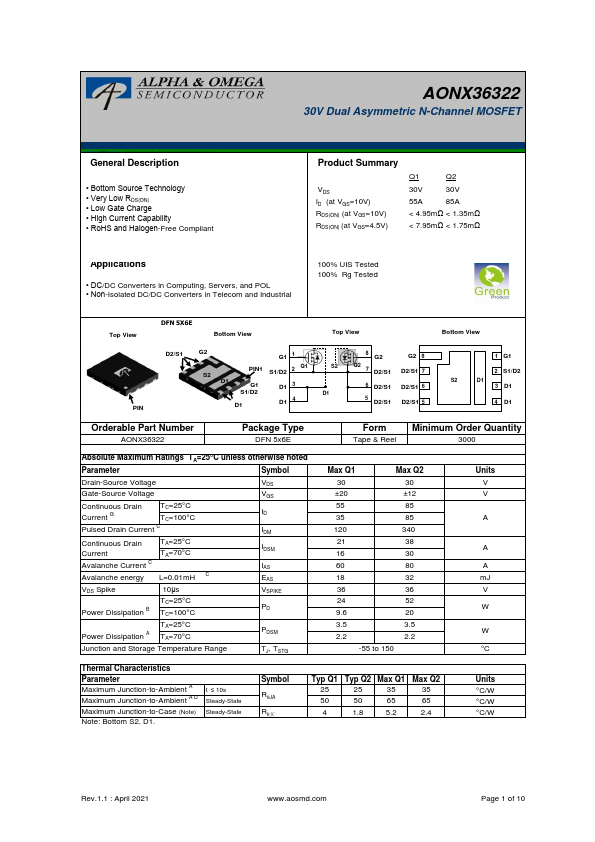
• Bottom Source Technology • Very Low RDS(ON) • Low Gate Charge • High Current Capability • RoHS and Halogen-Free Compliant Product Summary VDS ID (at VGS=10V) RDS(ON) (at VGS=10V) RDS(ON) (at VGS=4.5V) Q1 Q2 30V 30V 55A 85A < 4.95mΩ < 1.35mΩ < 7.95mΩ < 1.75mΩ Applications • DC/DC Converters in Computing, Servers, and POL • Non-Isolated DC/DC Converters in Telecom and Industrial 100% UIS Tested 100% Rg Tested Top View DFN 5X6E Bottom View Top View Bottom View D2/S1 G2 G1 1 8 G2 G2 8 S2 PIN1 S1/D2 2 Q1 S2 Q2 7 D2/S1 D2/S1 7 D1 G1 D1 3 6 D2/S1 D2/S1 6 S1/D2 D1 PIN D1 D1 4 5 D2/S1 D2/S1 5 1 G1 2 S1/D2 S2 D1 3 D1 4 D1 Orderable Part Number AONX36322 Package Type DFN 5x6E Form Minimum Order Quantity Tape & Reel 3000 Absolute Maximum Ratings TA=25°C unless otherwise noted Parameter Symbol Drain-Source Voltage VDS Gate-Source Voltage VGS Continuous Drain Current G TC=25°C TC=100°C ID Pulsed Drain Current C IDM Continuous Drain Current TA=25°C TA=70°C IDSM Avalanche Current C IAS Avalanche energy L=0.01mH C EAS VDS Spike Power Dissipation B 10μs TC=25°C TC=100°C VSPIKE PD TA=25°C Power Dissipation A TA=70°C PDSM Junction and Storage Temperature Range TJ, TSTG Max Q1 Max Q2 30 30 ±20 ±12 55 85 35 85 120 340 21 38 16 30 60 80 18 32 36 36 24 52 9.6 20 3.5 3.5 2.2 2.2 -55 to 150 Units V V A A A mJ V W W °C Thermal Characteristics Parameter Maximum Junction-to-Ambient A Maximum Junction-to-Ambient A D Maximum Junction-to-Case (Note) Note: Bottom S2, D1.
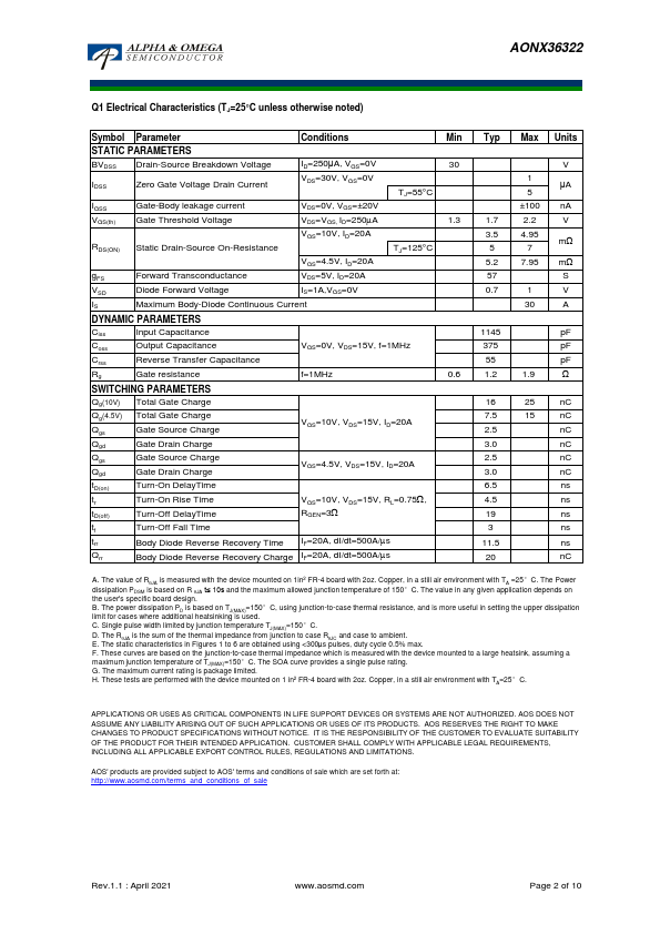
t ≤ 10s Steady-State Steady-State Symbol RqJA RqJC Typ Q1 25 50 4 Typ Q2 25 50 1.8 Max Q1 35 65 5.2 Max Q2 35 65 2.4 Units °C/W °C/W °C/W Rev.1.1 : April 2021 www.aosmd.com Page 1 of 10 AONX36322 0 Q1 Electrical Characteristics (TJ=25°C unless otherwise noted) Symbol Parameter Conditions Min STATIC PARAMETERS BVDSS Drain-Source Breakdown Volt
AONX36322 30V Dual Asymmetric N-Channel MOSFET General.
| Part Number | Description |
|---|---|
| AONX36320 | 30V Dual Asymmetric N-Channel MOSFET |
| AONX36324 | 30V Dual Asymmetric N-Channel MOSFET |
| AONX38168 | 25V Dual Asymmetric N-Channel MOSFET |
| AON1605 | 20V P-Channel MOSFET |
| AON1606 | 20V N-Channel MOSFET |
| AON1610 | 20V N-Channel MOSFET |
| AON1611 | P-Channel MOSFET |
| AON1620 | 12V N-Channel MOSFET |
| AON1634 | N-Channel MOSFET |
| AON2240 | 40V N-Channel MOSFET |