Datasheet Details
| Part number | AOP610 |
|---|---|
| Manufacturer | Alpha & Omega Semiconductors |
| File Size | 177.40 KB |
| Description | MOSFET |
| Datasheet |
 AOP610 Datasheet AOP610 Datasheet
|
|
|
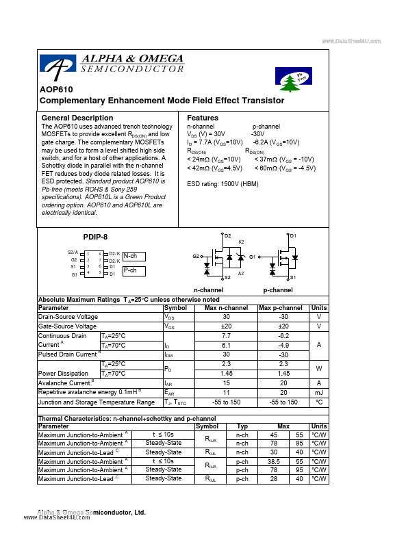
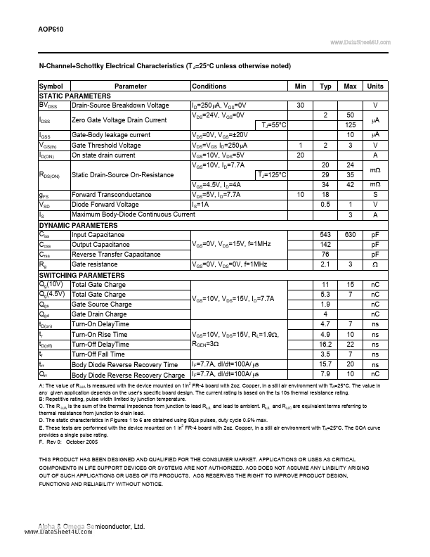
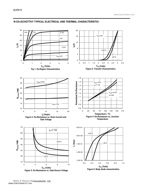
The AOP610 uses advanced trench technology MOSFETs to provide excellent RDS(ON) and low gate charge.
The complementary MOSFETs may be used to form a level shifted high side switch, and for a host of other applications.
| Part number | AOP610 |
|---|---|
| Manufacturer | Alpha & Omega Semiconductors |
| File Size | 177.40 KB |
| Description | MOSFET |
| Datasheet |
AOP610 Datasheet
|
|
|
|
| Part Number | Description |
|---|---|
| AOP611 | MOSFET |
| AOP600 | MOSFET |
| AOP601 | MOSFET |
| AOP605 | MOSFET |
| AOP605L | MOSFET |
| AOP606 | MOSFET |
| AOP607 | MOSFET |
| AOP608 | MOSFET |
| AOP609 | MOSFET |
| AOP800 | Dual N-Channel MOSFET |
The following content is an automatically extracted verbatim text from the original manufacturer datasheet and is provided for reference purposes only.