AO6605
AO6605 is MOSFET manufactured by Alpha & Omega Semiconductors.
Description
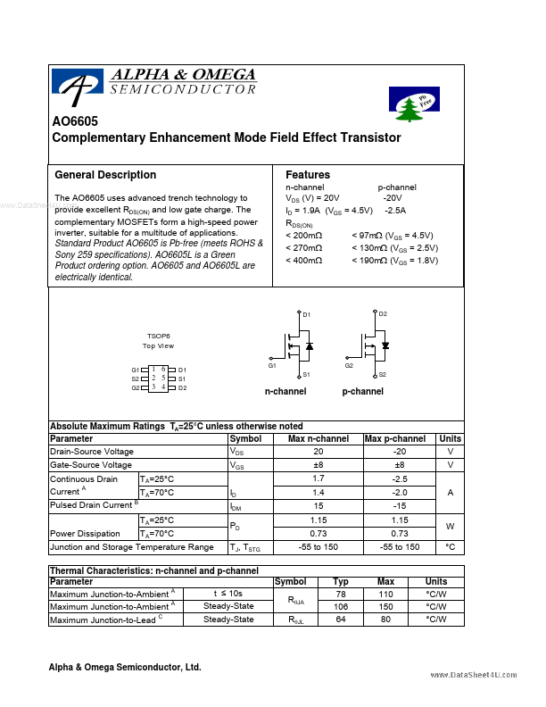
The AO6605 uses advanced trench technology to .. provide excellent RDS(ON) and low gate charge. The plementary MOSFETs form a high-speed power inverter, suitable for a multitude of applications. Standard Product AO6605 is Pb-free (meets ROHS & Sony 259 specifications). AO6605L is a Green Product ordering option. AO6605 and AO6605L are electrically identical.
Features n-channel p-channel -20V VDS (V) = 20V ID = 1.9A (VGS = 4.5V) -2.5A RDS(ON) < 200m Ω < 97mΩ (VGS = 4.5V) < 270m Ω < 130mΩ (VGS = 2.5V) < 400m Ω < 190mΩ (VGS = 1.8V)
D1 TSOP6 Top View G1 S2 G2 1 6 2 5 3 4 D1 S1 D2 G1 S1 G2
D2
S2 n-channel p-channel
Absolute Maximum Ratings TA=25°C unless otherwise noted Parameter Max n-channel Symbol VDS Drain-Source Voltage 20 Gate-Source Voltage Continuous Drain Current A Pulsed Drain Current Power Dissipation
Max p-channel -20 ±8 -2.5 -2.0 -15 1.15 0.73 -55 to 150
Units V V A
VGS TA=25°C TA=70°C TA=25°C TA=70°C ID IDM PD TJ, TSTG
±8 1.7 1.4 15 1.15 0.73 -55 to 150
W °C
Junction and Storage Temperature Range
Thermal Characteristics: n-channel and p-channel Parameter t ≤ 10s Maximum Junction-to-Ambient A Steady-State Maximum Junction-to-Ambient A Steady-State Maximum Junction-to-Lead C
Symbol RθJA RθJL
Typ 78 106 64
Max 110 150 80
Units °C/W °C/W °C/W
Alpha & Omega Semiconductor, Ltd.
N-channel MOSFET Electrical Characteristics (T J=25°C unless otherwise noted) Symbol Parameter Conditions ID=250µA, VGS=0V VDS=16V, VGS=0V TJ=55°C VDS=0V, VGS=±8V VDS=VGS ID=250µA VGS=4.5V, VDS=5V VGS=4.5V, ID=1.9A Static Drain-Source On-Resistance TJ=125°C VGS=2.5V, ID=1.6A VGS=1.8V, ID=1.3A g FS VSD IS Forward Transconductance VDS=5V, ID=1.9A Diode Forward Voltage IS=1A,VGS=0V Maximum Body-Diode Continuous Current 0.5 5 165 230 225 325 2.8 0.88 1 0.4 101 VGS=0V, VDS=10V, f=1MHz VGS=0V, VDS=0V, f=1MHz 17 14 3 1.6 VGS=4.5V, VDS=10V, ID=1.9A 0.2 0.4 3.2 VGS=5V, VDS=10V, RL=5.3Ω, RGEN=3Ω IF=1.9A, d I/dt=100A/µs 4 15.5 2.4 6.7 1.6 16 4 2 125 200 280...