AO6700
AO6700 is N-Channel MOSFET manufactured by Alpha & Omega Semiconductors.
Description
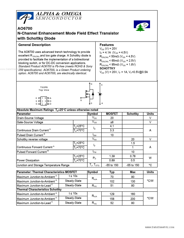
The AO6700 uses advanced trench technology to provide excellent R DS(ON) and low gate charge. A Schottky diode is provided to facilitate the implementation of a bidirectional blocking switch, or for DC-DC conversion applications. Standard Product AO6700 is Pb-free (meets ROHS & Sony .. 259 specifications). AO6700L is a Green Product ordering option. AO6700 and AO6700L are electrically identical.
Features
VDS (V) = 20V ID = 4.1A (VGS = 4.5V) RDS(ON) < 50mΩ (VGS = 4.5V) RDS(ON) < 65mΩ (VGS = 2.5V) RDS(ON) < 95mΩ (VGS = 1.8V) SCHOTTKY VDS (V) = 20V, IF = 1A, VF<0.5V@0.5A
TSOP6 Top View K S G A D D
1 6 2 5 3 4
Absolute Maximum Ratings TA=25°C unless otherwise noted Parameter Symbol VDS Drain-Source Voltage Gate-Source Voltage TA=25°C Continuous Drain Current Pulsed Drain Current
MOSFET 20 ±8 4.1 3.3 10
Schottky
Units V V A
VGS TA=70°C ID IDM VKA TA=25°C
Schottky reverse voltage Continuous Forward Current Pulsed Forward Current Power Dissipation Junction and Storage Temperature Range Parameter: Thermal Characteristics MOSFET t ≤ 10s Maximum Junction-to-Ambient A Maximum Junction-to-Ambient
TA=70°C TA=25°C TA=70°C
IF IFM PD TJ, TSTG Symbol RθJA RθJL RθJA RθJL 1.39 0.89 -55 to 150 Typ 70 102 51 129 158 52
20 1.5 1 10 0.78 0.5 -55 to 150 Max 90 130 80 160 200 80
W °C Units °C/W
Steady-State Steady-State t ≤ 10s Steady-State Steady-State
Maximum Junction-to-Lead Thermal Characteristics Schottky Maximum Junction-to-Ambient A Maximum Junction-to-Ambient Maximum Junction-to-Lead
°C/W
Electrical Characteristics (TJ=25°C unless otherwise noted) Symbol Parameter Conditions ID=250µA, VGS=0V VDS=16V, VGS=0V TJ=55°C VDS=0V, VGS=±8V VDS=VGS ID=250µA VGS=4.5V, VDS=5V VGS=4.5V, ID=4.1A
.. RDS(ON)
Min 20
Typ
Max
Units V
STATIC PARAMETERS BVDSS Drain-Source Breakdown Voltage IDSS IGSS VGS(th) ID(ON) Zero Gate Voltage Drain Current Gate-Body leakage current Gate Threshold Voltage On state drain current
1 5 100...