CEH2305 Overview
CEH2305 P-Channel Enhancement Mode Field Effect Transistor PRELIMINARY.
CEH2305 Key Features
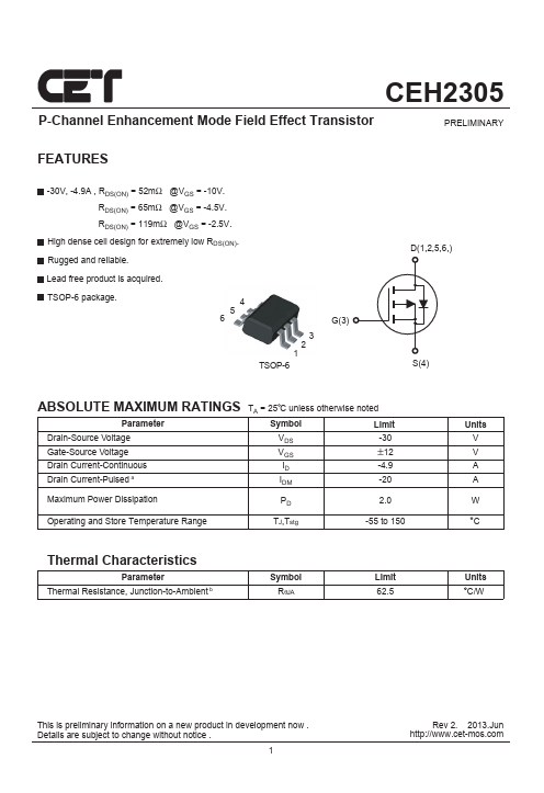
- 30V, -4.9A , RDS(ON) = 52mΩ @VGS = -10V. RDS(ON) = 65mΩ @VGS = -4.5V. RDS(ON) = 119mΩ @VGS = -2.5V
| Part number | CEH2305 |
|---|---|
| Datasheet | CEH2305-CET.pdf |
| File Size | 418.35 KB |
| Manufacturer | CET |
| Description | P-Channel Enhancement Mode Field Effect Transistor |
|
|
CEH2305 P-Channel Enhancement Mode Field Effect Transistor PRELIMINARY.