CTLM17NS10-R3
CTLM17NS10-R3 is N-Channel MOSFET manufactured by CT Micro.
CTLM17NS10-R3 N-Channel Enhancement MOSFET
Features
- Drain-Source Breakdown Voltage VDSS 100 V
- Drain-Source On-Resistance
RDS(ON) 3Ω, at VGS= 10V, ID= 100m A RDS(ON) 3Ω, at VGS= 4.5V, ID= 100m A
℃- Continuous Drain Current at TA=25 ID =0.17A
- Advanced high cell density Trench Technology
- Ro HS pliance & Halogen Free
Description
The CTLM17NS10-R3 is the N-Channel logic enhancement mode power field effect transistors are produced using high cell density, DMOS trench technology. This high density process is especially tailored to minimize on-state resistance.
Applications
- Power Management
- LCD Display inverter
- DC/DC Converter
- Load Switch
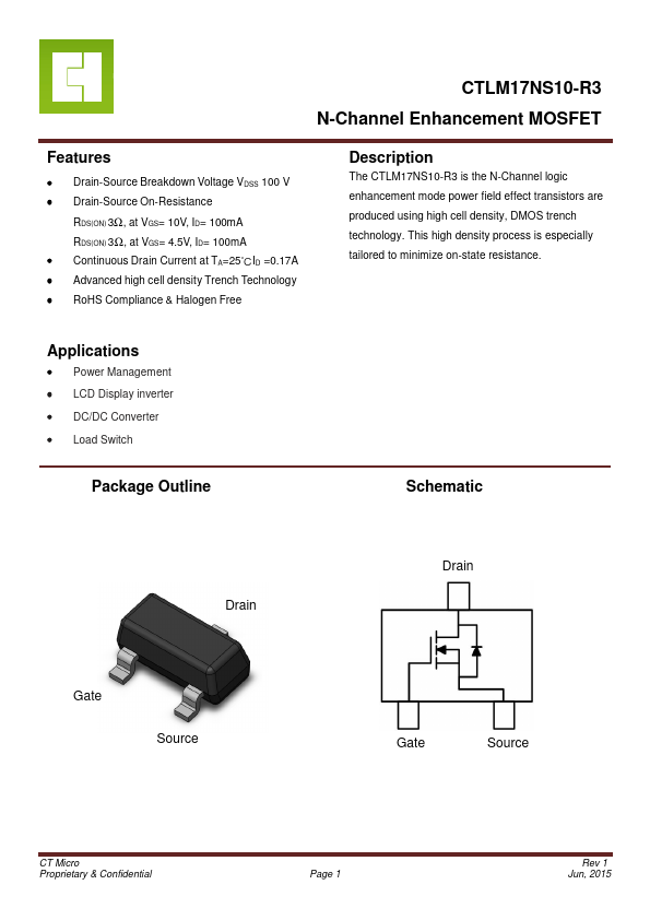
Package Outline
Schematic
Drain
Drain
Gate
Source
Gate
Source
CT Micro Proprietary & Confidential
Page 1
Rev 1 Jun, 2015
CTLM17NS10-R3 N-Channel Enhancement...