PE8810C
Overview
The PE8810C uses advanced trench technology to provide excellent RDS(ON) and low gate charge. It can be used in a wide variety of applications.
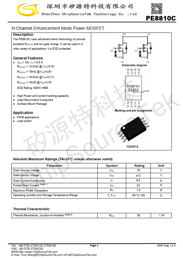
- VDS = 18V, ID = 8.5 A RDS(ON) < 13.5mΩ @ VGS=4.5V Schematic diagram RDS(ON) < 15mΩ @ VGS=3.8V RDS(ON) < 16.5mΩ @ VGS=3.1V RDS(ON) < 18mΩ @ VGS=2.5V ESD Rating: 4000V HBM
- High Power and current handing capability
- Lead free product is acquired
- Surface Mount Package k Application e
- PWM applications
- Load switch Marking and pin assignment rceT TSSOP-8 ou Absolute Maximum Ratings (TA=25℃ unless otherwise noted) S Drain-Source Voltage Parameter ip Gate-Source Voltage Drain Current-Continuous h Pulsed Drain Current (Note 1) C Maximum Power Dissipation Symbol