CY2DL814
CY2DL814 is 1:4 Clock Fanout Buffer manufactured by Cypress.
Link™ Series CY2DL814
1:4 Clock Fanout Buffer
Features
- -
- - Low-voltage operation VDD = 3.3V 1:4 Fanout Single-input configurable for
- LVDS, LVPECL, or LVTTL
- Four differential pairs of LVDS outputs Drives 50- or 100-ohm load (selectable) Low input capacitance Low output skew Does not exceed Bellcore 802.3 standards Operation at ⇒ 350 MHz
- 700 Mbps Low propagation delay Typical (tpd < 4 ns) Industrial versions available Packages available include TSSOP/SOIC
Description
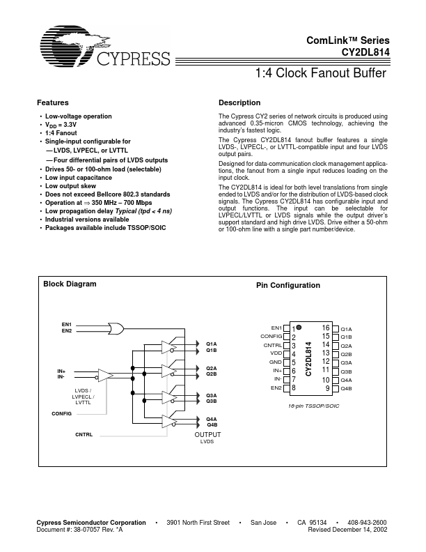
The Cypress CY2 series of network circuits is produced using advanced 0.35-micron CMOS technology, achieving the industry’s fastest logic. The Cypress CY2DL814 fanout buffer Features a single LVDS-, LVPECL-, or LVTTL-patible input and four LVDS output pairs. Designed for data-munication clock management applications, the fanout from a single input reduces loading on the input clock. The CY2DL814 is ideal for both level translations from single ended to LVDS and/or for the distribution of LVDS-based clock signals. The Cypress CY2DL814 has configurable input and output functions. The input can be selectable for LVPECL/LVTTL or LVDS signals while the output driver ’s support standard and high drive LVDS. Drive either a 50-ohm or 100-ohm line with a single part number/device.
- -
- -
- -
- -
Block Diagram
Pin Configuration
EN1 EN2 Q1A Q1B
EN1 CONFIG CNTRL VDD GND IN+ INEN2
Q3A Q3B
IN+ INLVDS / LVPECL / LVTTL CONFIG
Q2A Q2B
1 2 3 4 5 6 7 8
16 15 14 13 12 11 10 9
Q1A Q1B Q2A Q2B Q3A Q3B Q4A Q4B
16-pin TSSOP/SOIC
Q4A Q4B CNTRL
OUTPUT
LVDS
Cypress Semiconductor Corporation Document #: 38-07057 Rev.
-...