CY2DL818
CY2DL818 is 1:8 Clock Fanout Buffer manufactured by Cypress.
1:8 Clock Fanout Buffer
Features
- -
- -
- -
- -
- -
- -
- Low voltage operation VDD = 3.3V 1:8 fanout Single-input-configurable for LVDS, LVPECL, or LVTTL 8 pair of LVDS Outputs Drives either a 50-ohm or 100-ohm load (selectable) Low input capacitance Low output skew Low propagation delay Typical (tpd < 4 ns) Packages available include: TSSOP Does not exceed Bellcore 802.3 standards Operation at => 350 MHz
- 700 Mbps
Description
This Cypress series of network circuits is produced using advanced 0.35-micron CMOS technology, achieving the industry’s fastest logic. The Cypress CY2DL818 fanout buffer Features a single LVDS or a single-ended LVTTL-patible input and eight LVDS output pairs. Designed for data munications clock management applications, the large fanout from a single input reduces loading on the input clock. The Cypress CY2DL818 is ideal for both level translations from single-ended to LVDS and/or for the distribution of LVDS-based clock signals. The Cypress CY2DL818 has configurable input and output functions. The input can be selectable for LVCMOS/LVTTL, LVPECL, or LVDS signals, while the output drivers support standard and high-drive LVDS. Drive either a 50-ohm or 100-ohm line with a single part number/device.
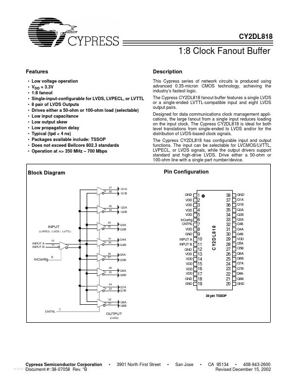
Block Diagram
37 36
Pin Configuration
Q1A Q1B
35 34
Q2A Q2B
(LVPECL / LVDS / LVTTL) 10 11 28 27 31 30
Q4A Q4B Q5A Q5B Q6A Q6B
INPUT A INPUT B
In Config
26 25
24 23
VDD GND INPUT A INPUT B GND VDD VDD VDD VDD VDD GND GND
CY2DL 818
INPUT
33 32
Q3A Q3B
GND VDD VDD VDD VDD In Config...