Datasheet4U Logo Datasheet4U.com

CY7C1347D - 128K x 36 Synchronous-Pipelined Cache SRAM

Datasheet Summary

Description

This Cypress Synchronous Burst SRAM employs high-speed, low-power CMOS designs using advanced triple-layer polysilicon, double-layer metal technology.

Each memory cell consists of four transistors and two high-valued resistors.

Features

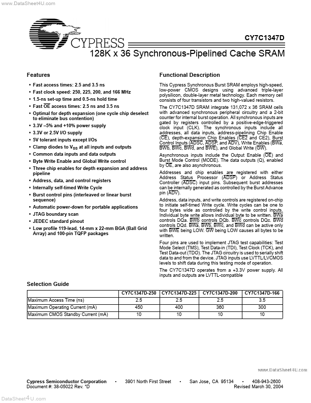
  • Fast access times: 2.5 and 3.5 ns.
  • Fast clock speed: 250, 225, 200, and 166 MHz.
  • 1.5-ns set-up time and 0.5-ns hold time.
  • Fast OE access times: 2.5 ns and 3.5 ns.
  • Optimal for depth expansion (one cycle chip deselect to eliminate bus contention).
  • 3.3V.
  • 5% and +10% power supply.
  • 3.3V or 2.5V I/O supply.
  • 5V tolerant inputs except I/Os.
  • Clamp diodes to VSS at all inputs and outputs.
  • Common data inputs.

📥 Download Datasheet

Datasheet preview – CY7C1347D

Datasheet Details

Part number CY7C1347D
Manufacturer Cypress Semiconductor
File Size 574.92 KB
Description 128K x 36 Synchronous-Pipelined Cache SRAM
Datasheet download datasheet CY7C1347D Datasheet
Additional preview pages of the CY7C1347D datasheet.
Other Datasheets by Cypress Semiconductor

Full PDF Text Transcription

Click to expand full text
www.DataSheet4U.com CY7C1347D 128K x 36 Synchronous-Pipelined Cache SRAM Features • Fast access times: 2.5 and 3.5 ns • Fast clock speed: 250, 225, 200, and 166 MHz • 1.5-ns set-up time and 0.5-ns hold time • Fast OE access times: 2.5 ns and 3.5 ns • Optimal for depth expansion (one cycle chip deselect to eliminate bus contention) • 3.3V –5% and +10% power supply • 3.3V or 2.
Published: |