Datasheet4U Logo Datasheet4U.com
Cypress (now Infineon) logo

CY7C1418AV18 Datasheet

Manufacturer: Cypress (now Infineon)
CY7C1418AV18 datasheet preview

CY7C1418AV18 Details

Part number CY7C1418AV18
Datasheet CY7C1418AV18 CY7C1416AV18 Datasheet (PDF)
File Size 287.10 KB
Manufacturer Cypress (now Infineon)
Description (CY7C14xxAV18) 36-Mbit DDR-II SRAM 2-Word Burst Architecture
CY7C1418AV18 page 2 CY7C1418AV18 page 3

CY7C1418AV18 Overview

The DDR-II consists of an SRAM core with advanced synchronous peripheral circuitry and a 1-bit burst counter. Addresses for Read and Write are latched on alternate rising edges of the input (K) clock. Write data is registered on the rising edges of both K.

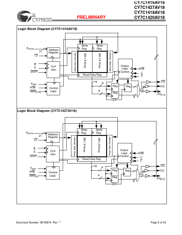
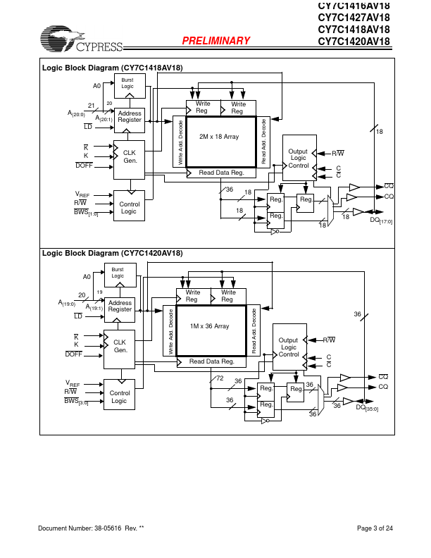
CY7C1418AV18 Key Features

  • 250-MHz clock for high bandwidth
  • 2-Word burst for reducing address bus frequency
  • Double Data Rate (DDR) interfaces (data transferred at 500 MHz) @ 250 MHz
  • Two input clocks (K and K) for precise DDR timing
  • SRAM uses rising edges only
  • Two output clocks (C and C) account for clock skew and flight time mismatching
  • Echo clocks (CQ and CQ) simplify data capture in high-speed systems
  • Synchronous internally self-timed writes
  • 1.8V core power supply with HSTL inputs and outputs
  • Variable drive HSTL output buffers

CY7C1418AV18 Distributor

Cypress (now Infineon) Datasheets

More from Cypress (now Infineon)

Datasheet4U Logo
Since 2006. D4U Semicon. About Datasheet4U Contact Us Privacy Policy Purchase of parts