MJD117 Overview
Description
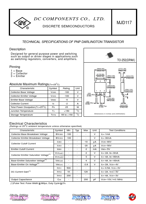
Designed for general purpose power and switching such as output or driver stages in applications such as switching regulators, converters, and amplifiers. Pinning 1 = Base 2 = Collector 3 = Emitter Characteristic Symbol Rating Collector-Base Voltage VCBO -100 Collector-Emitter Voltage VCEO -100 Emitter-Base Voltage VEBO -5 Collector Current Total Power Dissipation(TC=25oC) IC PD -2 25 Junction Temperature TJ +150 Storage Temperature TSTG -55 to +150 Unit V V V A W oC oC TO-252(DPAK) .268(6.80) .252(6.40) .217(5.50) .205(5.20) 2 .063(1.60) .055(1.40) .077(1.95) .065(1.65) .022(0.55) .018(0.45) 1 .035 (0.90) Max .032 Max (0.80) .228(5.80) .213(5.40) 23 .110(2.80) .087(2.20) .091 (2.30) Typ .059(1.50) .035(0.90) .024(0.60) .018(0.45) Dimensions in inches and (millimeters).