FDMA1027P
Overview
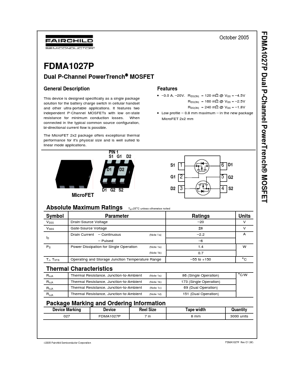
This device is designed specifically as a single package solution for the battery charge switch in cellular handset and other ultra-portable applications. It features two independent P-Channel MOSFETs with low on-state resistance for minimum conduction losses.
- -3.0 A, -20V. RDS(ON) = 120 mΩ @ VGS = -4.5V RDS(ON) = 160 mΩ @ VGS = -2.5V RDS(ON) = 240 mΩ @ VGS = -1.8V
- Low profile - 0.8 mm maximum - in the new package MicroFET 2x2 mm 1 2 3 6 5 4 D1 G2 S2 D1 G2 S2 MicroFET