FEATURES
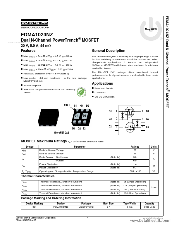
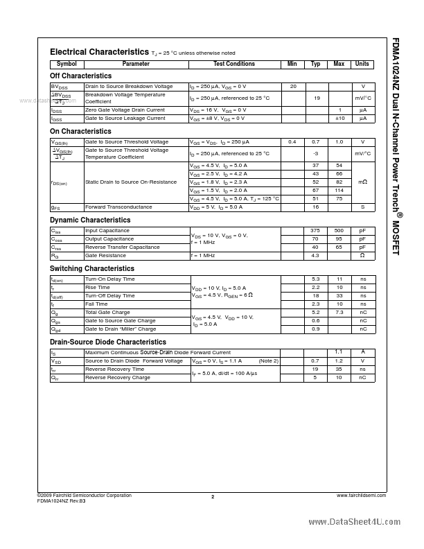
Max rDS(on) = 54 mΩ at VGS = 4.5 V, ID = 5.0 A Max rDS(on) = 66 mΩ at VGS = 2.5 V, ID = 4.2 A Max rDS(on) = 82 mΩ at VGS = 1.8 V, ID = 2.3 A Max rDS(on) = 114 mΩ at VGS = 1.5 V, ID = 2.0 A GENERAL DESCRIPTION
The MicroFET 2X2 package offers exceptional thermal performance for its physical size and is well suited to linear mode applications. HBM ESD protection level = 1.6 kV (Note 3) Low profile - 0.8 mm maximum - in the new package MicroFET 2x2 mm RoHS Compliant Free from halogenated compounds and antimony oxides APPLICATIONS
Baseband Switch Loadswitch DC-DC Conversion PIN 1 S1 G1 D2 S1 1 2 3 6 5 4 D1 G2 S2 D1 D2 G1 D2 D1 MicroFET 2x2 G2 S2 MOSFET MAXIMUM RATINGS
TA = 25 °C unless otherwise noted Symbol VDS VGS ID PD TJ, TSTG Parameter Drain to Source Voltage Gate to Source Voltage Drain Current -Continuous -Pulsed Power Dissipation Power Dissipation Operating and Storage Junction Temperature Range (Note 1a) (Note 1b) (Note 1a) Ratings 20 ±8 5.0 6.0 1.4 0... Fairchild Semiconductor