FDS6673BZ
Overview
- Max rDS(on) = 7.8mΩ, VGS = -10V, ID = -14.5A
- Max rDS(on) = 12mΩ, VGS = -4.5V, ID = -12A
- Extended VGS range (-25V) for battery applications
- HBM ESD protection level of 6.5kV typical (note 3)
- High performance trench technology for extremely low rDS(on)
- High power and current handling capability
- RoHS compliant
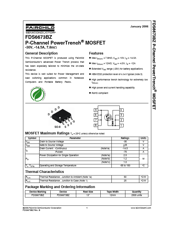
- 5 6 4 3 2 1 SO-8 S S S G 7 8 MOSFET Maximum Ratings TA = 25°C unless otherwise noted Symbol VDS VGS ID PD TJ, TSTG Operating and Storage Temperature Parameter Drain to Source Voltage Gate to Source Voltage Drain Current -Continuous -Pulsed Power Dissipation for Single Operation (Note1a) (Note1b) (Note1c) (Note1a) Ratings -30 ±25 -14.5 -75 2.5 1.2 1.0 -55 to 150 °C W Units V V A A Thermal Characteristics RθJA RθJC Thermal Resistance , Junction to Ambient (Note 1a) Thermal Resistance , Junction to Case (Note 1) 50 25 °C/W °C/W Package Marking and Ordering Information