FDS8842NZ
FDS8842NZ is N-Channel MOSFET manufactured by Fairchild Semiconductor.
FDS8842NZ N-Channel Power Trench® MOSFET
N-Channel Power Trench® MOSFET
February 2009
40 V, 14.9 A, 7.0 mΩ Features
General Description
- Max r DS(on) = 7.0 mΩ at VGS = 10 V, ID = 14.9 A
- Max r DS(on) = 11.6 mΩ at VGS = 4.5 V, ID = 11.6 A
- HBM ESD protection level of 4.4 k V typical(note 3)
- High performance trench technology for extremely low r DS(on) and fast switching
- High power and current handling capability
- Termination is Lead-free and Ro HS pliant
The FDS8842NZ has been designed to minimize losses in power conversion application. Advancements in both silicon and package technologies have been bined to offer the lowest r DS(on) while maintaining excellent switching performance.
Applications
- Synchronous Buck for Notebook Vcore and Server
- Notebook Battery
- Load Switch
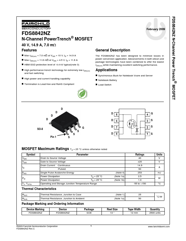
SO-8
Pin 1
MOSFET Maximum Ratings TA = 25 °C unless otherwise noted
Symbol VDS VGS
TJ, TSTG
Parameter
Drain to Source Voltage
Gate to Source Voltage
Drain Current -Continuous
-Pulsed
Single Pulse Avalanche Energy
Power Dissipation
TA = 25 °C
Power...