Datasheet4U.com
🌙
FDS9934C Datasheet | Fairchild Semiconductor
Part:
FDS9934C
Description:
MOSFET
Category:
MOSFET
Manufacturer:
Fairchild Semiconductor
Size:
182.01 KB
FDS9934C Datasheet (PDF) Download
Related FDS9934C Datasheets
FDS9936A Dual N-Channel Enhancement Mode Field Effect Transistor
FDS9933 Dual P-Channel 2.5V Specified PowerTrench MOSFET
FDS9933A Dual P-Channel 2.5V Specified PowerTrench MOSFET
FDS9933BZ Dual P-Channel 2.5V Specified PowerTrench MOSFET
Fairchild Semiconductor
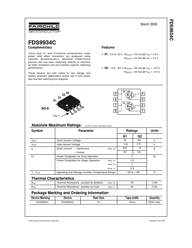
FDS9934C
Key Features
Q1: 6.5 A, 20 V. RDS(ON) = 30 mΩ @ VGS = 4.5 V RDS(ON) = 43 mΩ @ VGS = 2.5 V
Datasheets by Manufacturer
Part Number
Manufacturer
Description
FDS9933A
onsemi
Dual P-Channel MOSFET
×
Close