IRF610B Overview
Key Specifications
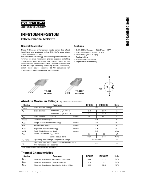
Package: TO-220
Max Operating Temp: 150 °C
Description
These N-Channel enhancement mode power field effect transistors are produced using Fairchild’s proprietary, planar, DMOS technology. This advanced technology has been especially tailored to minimize on-state resistance, provide superior switching performance, and withstand high energy pulse in the avalanche and commutation mode.