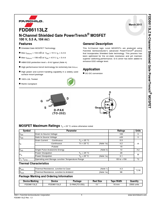
FDD86113LZ Description
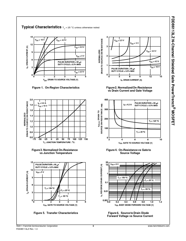
Shielded Gate MOSFET Technology Max rDS(on) = 104 mΩ at VGS = 10 V, ID = 4.2 A Max rDS(on) = 156 mΩ at VGS = 4.5 V, ID = 3.4 A HBM ESD protection level > 6 kV typical (Note 4) This N-Channel logic Level MOSFETs are produced using Fairchild Semiconductor‘s advanced PowerTrench® process that incorporates Shielded Gate technology. This process has been optimized for the on-state resistance and yet maintain...
FDD86113LZ Key Features
- Shielded Gate MOSFET Technology
- Max rDS(on) = 104 mΩ at VGS = 10 V, ID = 4.2 A
- Max rDS(on) = 156 mΩ at VGS = 4.5 V, ID = 3.4 A
- HBM ESD protection level > 6 kV typical (Note 4)
- High performance trench technology for extremely low rDS(on)
- High power and current handling capability in a widely used surface mount package
- DC-DC conversion
- 100% UIL Tested
- RoHS pliant
- Pulsed