FPD3000
FPD3000 is 2W POWER PHEMT manufactured by Filtronic Compound Semiconductors.
FEATURES
- 32.5 d Bm Linear Output Power at 12 GHz
- 6.5 d B Power Gain at 12 GHz
- 8 d B Maximum Stable Gain at 12 GHz
- 42 d Bm Output IP3
- 30% Power-Added Efficiency
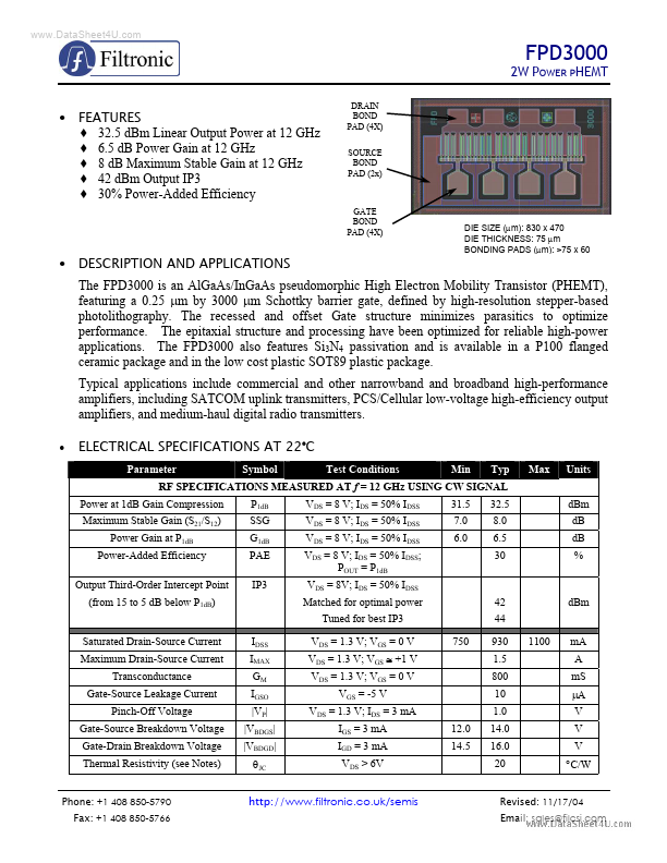
DRAIN BOND PAD (4X) SOURCE BOND PAD (2x)
GATE BOND PAD (4X)
- DESCRIPTION
AND APPLICATIONS
DIE SIZE (µm): 830 x 470 DIE THICKNESS: 75 µm BONDING PADS (µm): >75 x 60
The FPD3000 is an Al Ga As/In Ga As pseudomorphic High Electron Mobility Transistor (PHEMT), featuring a 0.25 µm by 3000 µm Schottky barrier gate, defined by high-resolution stepper-based photolithography. The recessed and offset Gate structure minimizes parasitics to optimize performance. The epitaxial structure and processing have been optimized for reliable high-power applications. The FPD3000 also features
Si3N4 passivation and is available in a P100 flanged ceramic package and in the low cost plastic SOT89 plastic package. Typical applications include mercial and other narrowband and broadband high-performance amplifiers, including SAT uplink transmitters, PCS/Cellular low-voltage high-efficiency output amplifiers, and medium-haul digital radio transmitters.
- ELECTRICAL SPECIFICATIONS AT 22°C
Parameter Power at 1d B Gain pression Maximum Stable Gain (S21/S12) Power Gain at P1d B Power-Added Efficiency Output Third-Order Intercept Point (from 15 to 5 d B below P1d B) Saturated Drain-Source Current Maximum Drain-Source Current Transconductance Gate-Source Leakage Current Pinch-Off Voltage Gate-Source Breakdown Voltage Gate-Drain Breakdown Voltage Thermal Resistivity (see Notes) IDSS IMAX GM IGSO |VP| |VBDGS| |VBDGD| θJC Symbol P1d B SSG G1d B PAE IP3 Test Conditions VDS = 8 V; IDS = 50% IDSS VDS = 8 V; IDS = 50% IDSS VDS = 8 V; IDS = 50% IDSS VDS = 8 V; IDS = 50% IDSS; POUT = P1d B VDS = 8V; IDS = 50% IDSS Matched for optimal power Tuned for best IP3 VDS = 1.3 V; VGS = 0 V VDS = 1.3 V; VGS ≅ +1 V VDS = 1.3 V; VGS = 0 V VGS = -5 V VDS = 1.3 V; IDS = 3 m A IGS = 3 m A IGD = 3 m A VDS > 6V 12.0 14.5 750 42 44 930 1.5 800 10 1.0 14.0 16.0...