FPD7612P70
FPD7612P70 is HI-FREQUENCY PACKAGED PHEMT manufactured by Filtronic Compound Semiconductors.
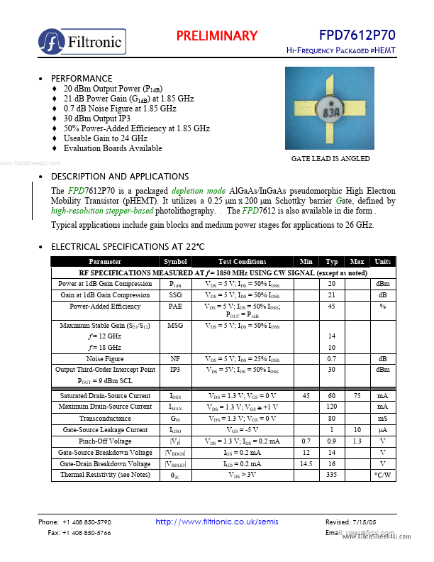
PLICATIONS The FPD7612P70 is a packaged depletion mode Al Ga As/In Ga As pseudomorphic High Electron Mobility Transistor (p HEMT). It utilizes a 0.25 µm x 200 µm Schottky barrier Gate, defined by high-resolution stepper-based photolithography. . The FPD7612 is also available in die form . Typical applications include gain blocks and medium power stages for applications to 26 GHz.
- ELECTRICAL SPECIFICATIONS AT 22°C
Parameter Power at 1d B Gain pression Gain at 1d B Gain pression Power-Added Efficiency Maximum Stable Gain (S21/S12) f = 12 GHz f = 18 GHz Noise Figure Output Third-Order Intercept Point POUT = 9 d Bm SCL Saturated Drain-Source Current Maximum Drain-Source Current Transconductance Gate-Source Leakage Current Pinch-Off Voltage Gate-Source Breakdown Voltage Gate-Drain Breakdown Voltage Thermal Resistivity (see Notes) IDSS IMAX GM IGSO |VP| |VBDGS| |VBDGD| θJC VDS = 1.3 V; VGS = 0 V VDS = 1.3 V; VGS ≅ +1 V VDS = 1.3 V; VGS = 0 V VGS = -5 V VDS = 1.3 V; IDS = 0.2 m A IGS = 0.2 m A IGD = 0.2 m A VDS > 3V 0.7 12 14.5 45 60 120 80 1 0.9 14 16 335 10 1.3 75 m A m A m S µA V V V °C/W NF IP3 VDS = 5 V; IDS = 25% IDSS VDS = 5V; IDS = 50% IDSS Symbol P1d B SSG PAE MSG Test Conditions VDS = 5 V; IDS = 50% IDSS VDS = 5 V; IDS = 50% IDSS VDS = 5 V; IDS = 50% IDSS; POUT = P1d B VDS = 5 V; IDS = 50% IDSS 14 10 0.7 30 d B d Bm Min Typ 20 21 45 Max Units d Bm d B % RF SPECIFICATIONS MEASURED AT f = 1850 MHz USING CW SIGNAL (except as noted)
Phone: +1 408 850-5790 Fax: +1 408 850-5766 http://.filtrionic.co.uk/semis
Revised: 7/15/05 Email: sales@filcsi.
PRELIMINARY
- ABSOLUTE MAXIMUM RATINGS1
Parameter Drain-Source Voltage Gate-Source Voltage Drain-Source Current Gate Current RF Input Power Channel ..
HI-FREQUENCY PACKAGED PHEMT
Symbol VDS VGS IDS IG PIN TCH TSTG PTOT p.
Test Conditions -3V < VGS < +0V 0V < VDS < +8V For VDS > 2V Forward or reverse current Under any acceptable bias state Under any acceptable bias state Non-Operating Storage See De-Rating Note below...