FPD1500DFN
FPD1500DFN is HIGH LINEARITY PACKAGED PHEMTT manufactured by Filtronic.
FEATURES
(1850MHZ):
- -
- -
- - 27 d Bm Output Power (P1d B) 18 d B Small-Signal Gain (SSG) 1.2 d B Noise Figure 42 d Bm Output IP3 45% Power-Added Efficiency Ro HS pliant (Directive 2002/95/EC)
Datasheet v2.1
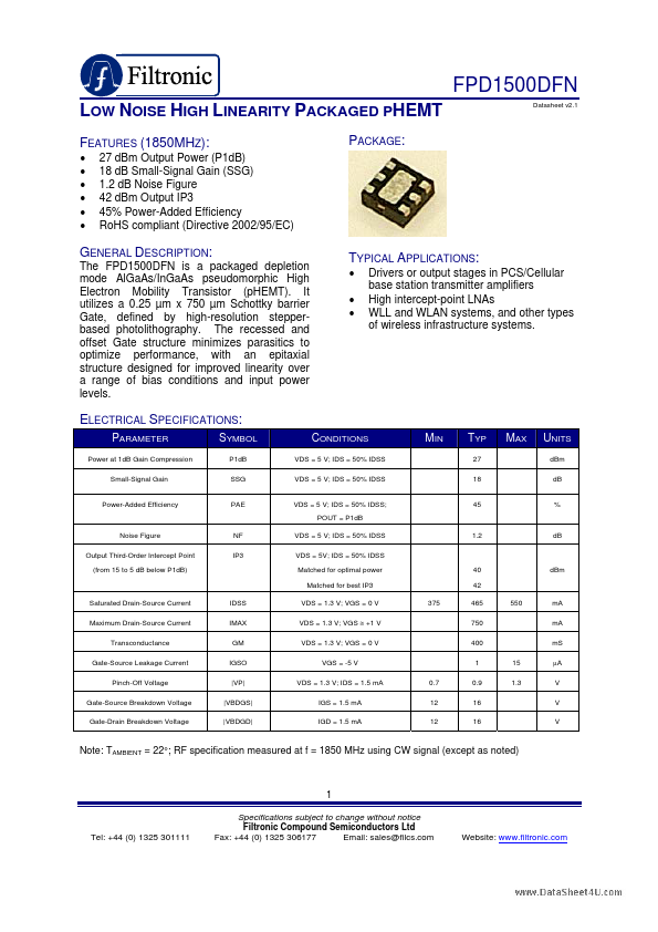
PACKAGE:
GENERAL DESCRIPTION
:
The FPD1500DFN is a packaged depletion mode Al Ga As/In Ga As pseudomorphic High Electron Mobility Transistor (p HEMT). It utilizes a 0.25 µm x 750 µm Schottky barrier Gate, defined by high-resolution stepperbased photolithography. The recessed and offset Gate structure minimizes parasitics to optimize performance, with an epitaxial structure designed for improved linearity over a range of bias conditions and input power levels.
TYPICAL APPLICATIONS:
- -
- Drivers or output stages in PCS/Cellular base station transmitter amplifiers High intercept-point LNAs WLL and WLAN systems, and other types of wireless infrastructure systems.
ELECTRICAL SPECIFICATIONS:
PARAMETER
Power at 1d B Gain pression Small-Signal Gain
SYMBOL
P1d B SSG
CONDITIONS
VDS = 5 V; IDS = 50% IDSS VDS = 5 V; IDS = 50% IDSS
27 18
UNITS d Bm d B
Power-Added Efficiency
VDS = 5 V; IDS = 50% IDSS; POUT = P1d B
%
Noise Figure Output Third-Order Intercept Point (from 15 to 5 d B below P1d B)
NF IP3
VDS = 5 V; IDS = 50% IDSS VDS = 5V; IDS = 50% IDSS Matched for optimal power Matched for best IP3
1.2 d B
40 42 375 465 750 400 1 0.7 12 12 0.9 16 16 15 1.3 550 d Bm
Saturated Drain-Source Current Maximum Drain-Source Current Transconductance Gate-Source Leakage Current Pinch-Off Voltage Gate-Source Breakdown Voltage Gate-Drain Breakdown Voltage
IDSS IMAX GM IGSO |VP| |VBDGS| |VBDGD|
VDS = 1.3 V; VGS = 0 V VDS = 1.3 V; VGS ≅ +1 V VDS = 1.3 V; VGS = 0 V VGS = -5 V VDS = 1.3 V; IDS = 1.5 m A IGS = 1.5 m A IGD = 1.5 m A m A m A m S μA V V V
Note: TAMBIENT = 22°; RF specification measured at f = 1850 MHz using CW signal (except as...