MRF6P27160HR6
MRF6P27160HR6 is RF Power Field Effect Transistor manufactured by Freescale Semiconductor.
Freescale Semiconductor Technical Data
MRF6P27160H Rev. 0, 1/2005
RF Power Field Effect Transistor
- Channel Enhancement
- Mode Lateral MOSFET
Designed for N
- CDMA base station applications with frequencies from 2600 to 2700 MHz. Suitable for TDMA, CDMA and multicarrier amplifier applicat i o n s . To b e u s e d i n C l a s s A B f o r P C N
- P C S / c e l l u l a r r a d i o a n d W L L applications.
- Typical Single
- Carrier N
- CDMA Performance: VDD = 28 Volts, IDQ = 2 x 900 m A, Pout = 35 Watts Avg., Full Frequency Band, IS
- 95 CDMA (Pilot, Sync, Paging, Traffic Codes 8 Through 13) Channel Bandwidth = 1.2288 MHz. Peak/Avg. = 9.8 d B @ 0.01% Probability on CCDF. Power Gain
- 14.6 d B Drain Efficiency
- 22.6% ACPR @ 885 k Hz Offset
- - 47.8 d Bc @ 30 k Hz Bandwidth
- Capable of Handling 10:1 VSWR, @ 28 Vdc, 2700 MHz, 160 Watts CW Output Power
- Characterized with Series Equivalent Large
- Signal Impedance Parameters
- Internally Matched, Controlled Q, for Ease of Use
- Qualified Up to a Maximum of 32 VDD Operation
- Integrated ESD Protection
- Lower Thermal Resistance Package
- Designed for Lower Memory Effects and Wide Instantaneous Bandwidth Applications
- Low Gold Plating Thickness on Leads, 40µ″ Nominal.
- In Tape and Reel. R6 Suffix = 150 Units per 56 mm, 13 inch Reel.
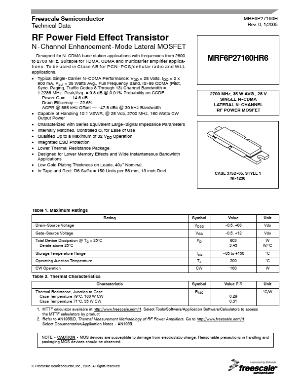
2700 MHz, 35 W AVG., 28 V SINGLE N
- CDMA LATERAL N
- CHANNEL RF POWER MOSFET
CASE 375D
- 05, STYLE 1 NI
- 1230
Table 1. Maximum Ratings
Rating Drain
- Source Voltage Gate
- Source Voltage Total Device Dissipation @ TC = 25°C Derate above 25°C Storage Temperature Range Operating Junction Temperature CW Operation Symbol VDSS VGS PD Tstg TJ CW Value
- 0.5, +68
- 0.5, +12 603 3.45
- 65 to +150 200 160 Unit Vdc Vdc W W/°C °C °C W
Table 2. Thermal Characteristics...