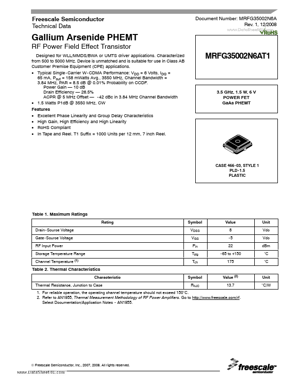
MRFG35002N6AT1
MRFG35002N6AT1 is Gallium Arsenide PHEMT RF Power Field Effect Transistor manufactured by Freescale Semiconductor.
Features
- Excellent Phase Linearity and Group Delay Characteristics
- High Gain, High Efficiency and High Linearity
- Ro HS pliant
- In Tape and Reel. T1 Suffix = 1000 Units per 12 mm, 7 inch Reel.
3.5 GHz, 1.5 W, 6 V POWER FET Ga As PHEMT
CASE 466
- 03, STYLE 1 PLD
- 1.5 PLASTIC
Table 1. Maximum Ratings
Rating Drain
- Source Voltage Gate
- Source Voltage RF Input Power Storage Temperature Range Channel Temperature
(1)
Symbol VDSS VGS Pin Tstg Tch
Value 8 -5 22
- 65 to +150 175
Unit Vdc Vdc d Bm °C °C
Table 2. Thermal Characteristics
Characteristic Thermal Resistance, Junction to Case Symbol RθJC Value (2) 13.7 Unit °C/W
1. For reliable operation, the operating channel temperature should not exceed 150°C. 2. Refer to AN1955, Thermal Measurement Methodology of RF Power Amplifiers. Go to http://.freescale./rf. Select Documentation/Application Notes
- AN1955.
© Freescale Semiconductor, Inc., 2007, 2008. All rights reserved.
MRFG35002N6AT1 1
RF Device Data Freescale Semiconductor
Table 3. ESD Protection Characteristics
Test Methodology Human Body Model (per JESD22
- A114) Machine Model (per EIA/JESD22
- A115) Charge Device Model (per JESD22
- C101) Class 1C (Minimum) A (Minimum) IV (Minimum) ..
Table 4. Moisture Sensitivity Level
Test Methodology Per JESD 22
- A113, IPC/JEDEC J
- STD
- 020 Rating 1 Package Peak Temperature 260 Unit °C
Table 5. Electrical Characteristics (TC = 25°C unless otherwise noted)
Characteristic Saturated Drain Current (VDS = 3.5 Vdc, VGS = 0 Vdc) Off State Leakage Current (VGS =
- 0.4 Vdc, VDS = 0 Vdc) Off State Drain Current (VDS = 6 Vdc, VGS =
- 2.5 Vdc) Off State Current (VDS = 28.5 Vdc, VGS =
- 2.5 Vdc)...