GSM2519
GSM2519 is MOSFET manufactured by Globaltech.
20V N&P Pair Enhancement Mode MOSFET
Product Description
GSM2519, N & P Pair enhancement mode MOSFET, uses Advanced Trench Technology to provide excellent RDS(ON), low gate charge. These devices are particularly suited for low voltage power management, and low in-line power loss are needed in mercial industrial surface mount applications.
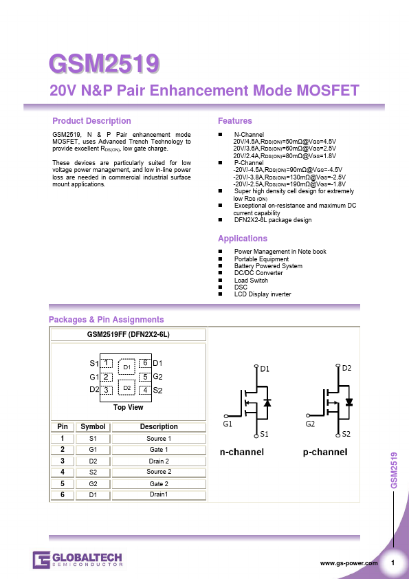
Packages & Pin Assignments
GSM2519FF (DFN2X2-6L)
Features
- N-Channel 20V/4.5A,RDS(ON)=50mΩ@VGS=4.5V 20V/3.6A,RDS(ON)=60mΩ@VGS=2.5V 20V/2.4A,RDS(ON)=80mΩ@VGS=1.8V
- P-Channel -20V/-4.5A,RDS(ON)=90mΩ@VGS=-4.5V -20V/-3.8A,RDS(ON)=130mΩ@VGS=-2.5V -20V/-2.5A,RDS(ON)=190mΩ@VGS=-1.8V
- Super high density cell design for extremely low RDS (ON)
- Exceptional on-resistance and maximum DC current capability
- DFN2X2-6L package design
Applications
- Power Management in Note book
- Portable Equipment
- Battery Powered System
- DC/DC Converter
- Load Switch
- DSC
- LCD Display inverter
Top View
Pin Symbol 1 S1 2 G1...