4AK27
4AK27 is Silicon N Channel MOS FET High Speed Power Switching manufactured by Hitachi Semiconductor.
Features
- Low on-resistance R DS(on) ≤ 0.15Ω, VGS = 10V, ID = 3.0A
- 4V gate drive devices.
- High density mounting
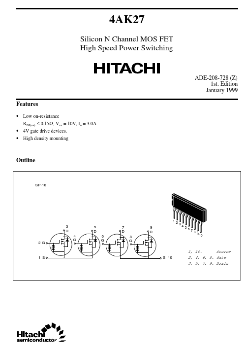
Outline
SP-10
3 D 2G 4 G
5 D 6 G
7 D 8 G
9 D
12 34 56 78 9 10
1 S
S 10
1, 10. Source 2, 4, 6, 8. Gate 3, 5, 7, 9. Drain
Absolute Maximum Ratings (Ta = 25°C)
Item Drain to source voltage Gate to source voltage Drain current Drain peak current Body-drain diode reverse drain current Avalanche current Avalanche energy1 Channel dissipation Channel dissipation Channel temperature Storage temperature Note: Symbol VDSS VGSS ID I D(pulse) I DR I AP EAR Pch(Tc=25˚C) Pch Tch Tstg
Note2 Note2 Note1
Ratings 60 ±20 5 20 5 5 2.1 28 4 150
- 55 to +150
Unit V V A A A A m J W W °C °C
1. PW ≤ 10 µs, duty cycle ≤ 1 % 2. 4 devices poeration 3. Value at Tch=25˚C, Rg ≥ 50 Ω
Electrical Characteristics (Ta = 25°C)
Item Drain to source breakdown voltage Gate to source breakdown voltage Zero gate voltege drain current Gate to source leak current Gate to source cutoff voltage Static drain to source on state resistance Static drain to source on state resistance Forward transfer admittance Input capacitance Output capacitance Reverse transfer capacitance Turn-on delay time Rise time Turn-off delay time Fall time Body- drain diode forward voltage Body- drain diode reverse recovery time Note: 4. Pulse test Symbol V(BR)DSS V(BR)GSS I DSS I GSS VGS(off) RDS(on) RDS(on) |yfs| Ciss Coss Crss t d(on) tr t d(off) tf VDF t rr Min 60 ±20
- - 1.0
- - 3.0
- -
- -
- -
- -
- Typ
- -
- -
- 0.12 0.15 5.5 390 190 45 10 42 90 55 1.0 60 Max
- - 100 ±10 2.25 0.15 0.2
- -
- -
- -
- -
- - Unit Test Conditions V V µA µA V Ω Ω S p F p F p F ns ns ns ns V ns I F = 5A, VGS = 0 I F = 5A, VGS = 0 di F/ dt =50A/µs I D = 10m A, VGS = 0 I G = ±100µA, VDS = 0 VDS = 50 V, VGS = 0 VGS = ±16V, VDS = 0 I D = 1m A, VDS = 10V I D = 3A, VGS = 10V Note4 I D = 3A, VGS = 4V Note4 I D = 3A, VDS = 10V Note4 VDS = 10V VGS = 0 f = 1MHz VGS = 10V, ID = 3A RL = 10Ω
Main Characteristics...