2SK3349
2SK3349 is N-Channel MOSFET manufactured by Hitachi Semiconductor.
Features
- Low on-resistance R DS = 2.8 Ω typ. (at VGS = 4 V , ID = 25 m A) R DS = 4.8 Ω typ. (at VGS = 2.5 V , I D = 10 m A)
- 2.5 V gate drive device
- Small package (SMPAK)
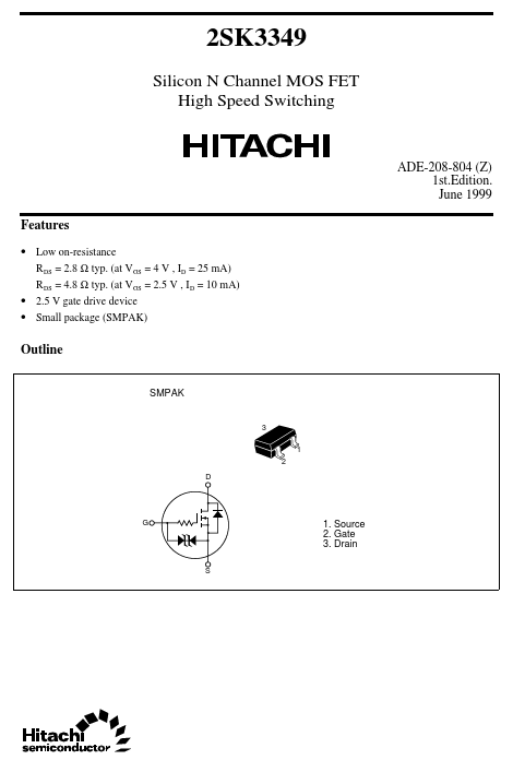
Outline
SMPAK
3 1 2 D
1. Source 2. Gate 3. Drain
Absolute Maximum Ratings (Ta = 25°C)
Item Drain to source voltage Gate to source voltage Drain current Drain peak current Body-drain diode reverse drain current Channel dissipation Channel temperature Storage temperature Note: Symbol VDSS VGSS ID I D(pulse) I DR Pch Tch Tstg
Note 2 Note1
Ratings 20 ±10 50 200 50 100 150
- 55 to +150
Unit V V m A m A m A m W °C °C
1. PW ≤ 10 µs, duty cycle ≤ 1% 2. Value on the alumina ceramic board (12.5x20x0.7 mm)
Electrical Characteristics (Ta = 25°C)
Item Drain to source breakdown voltage Gate to source breakdown voltage Gate to source leak current Zero gate voltege drain current Symbol V(BR)DSS V(BR)GSS I GSS I DSS Min 20 ±10
- - 0.8
- - 56
- -
- -
- -
- Typ
- -
- -
- 2.8 4.8 85 6 7 1.2 120 450 480 500 Max
- - ±5 1 1.8 3.6 7.2
- -
- -
- -
- - Unit V V µA µA V Ω Ω m S p F p F p F ns ns ns ns Test Conditions I D = 100 µA, VGS = 0 I G = ±100 µA, VDS = 0 VGS = ±8 V, VDS = 0 VDS = 20 V, VGS = 0 I D = 10 µA, VDS = 5 V
ID = 25 m A,VGS = 4 V Note 3 ID = 10 m A,VGS = 2.5 V Note 3 ID = 25 m A, VDS = 10 V Note 3
Gate to source cutoff voltage VGS(off) Static drain to source on state RDS(on) resistance Forward transfer admittance Input capacitance Output capacitance RDS(on) |yfs| Ciss Coss
VDS = 10 V VGS = 0 f = 1 MHz I D = 25 m A, VGS = 4 V RL = 400 Ω
Reverse transfer capacitance Crss Turn-on delay time Rise time Turn-off delay time Fall time Note: 3. Pulse test 4. Marking is DN t d(on) tr t d(off) tf
Main Characteristics
Power vs. Temperature Derating 200
- Pch (m W)
5 2 1.0 0.5 0.2 0.1 0.05 0.02 0.01 0.005 0.002...