3SK309
3SK309 is UHF RF Amplifier manufactured by Hitachi Semiconductor.
Features
- Capable of low voltage operation (VDS = 1.5 to 3 V)
- Excellent low noise characteristics (NF = 1.25 d B typ. at f = 900 MHz)
- High power gain (PG = 21.0 d B typ. at f = 900 MHz)
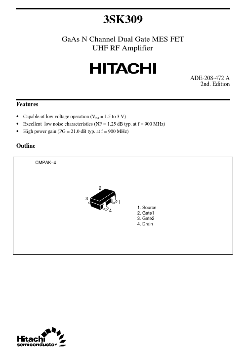
Outline
CMPAK- 4
2 3 4 1 1. Source 2. Gate1 3. Gate2 4. Drain
Absolute Maximum Ratings (Ta = 25°C)
Item Drain to source voltage Gate 1 to source voltage Gate 2 to source voltage Drain current Channel power dissipation Channel temperature Storage temperature Symbol VDS VG1S VG2S ID Pch Tch Tstg Ratings 6
- 4
- 4 18 100 125
- 55 to +125 Unit V V V m A m W °C °C
Electrical Characteristics (Ta = 25°C)
Item Gate 1 to cutoff current Gate 2 to cutoff current Symbol I G1SS I G2SS Min
- -
- 0.2
- 0.2 25 30 18
- -
- Typ
- -
- - 40 40 21 1.25 20 1.3 Max
- 20
- 20
- 1.5
- 1.5 60
- - 1.5
- - Unit µA µA V V m A m S d B d B d B d B Test conditions VG1S =
- 4 V VG2S = VDS = 0 VG2S =
- 4 V VG1S = VDS = 0 VDS = 3 V, VG2S = 0 I D = 100 µA VDS = 3 V, VG1S = 0 I D = 100 µA VDS = 3 V, VG1S = 0 VG2S = 0 VDS = 3 V, VG2S = 0 I D = 5 m A, f = 1 k Hz VDS = 3 V, VG2S = 0 I D = 5 m A, f = 900 MHz VDS = 1.5 V, VG2S = 0 I D = 3 m A, f = 900 MHz
Gate 1 to source cutoff voltage VG1S(off) Gate 2 to source cutoff voltage VG2S(off) Zero gate voltege drain current I DSS Forward transfer admittance Power gain Noise figure Power gain Noise figure Note: Marking is “XV- ” |yfs| PG NF PG NF
Main Characteristics
Maximum Channel Power Dissipation Curve 200 Channel Power Dissipation Pch (m W)
Typical Output Characteristics
- 0.4 V
- 0.5 V
- 0.6 V Pulse Test
- 0.7 V
Drain Current ID (m...