Datasheet Summary
4 Banks x 2M x 16bits Synchronous DRAM
DESCRIPTION
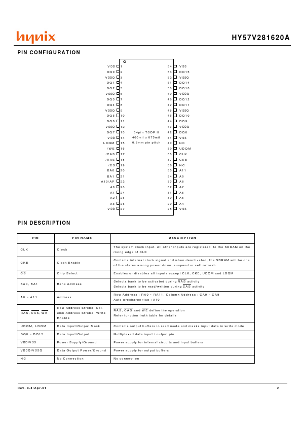
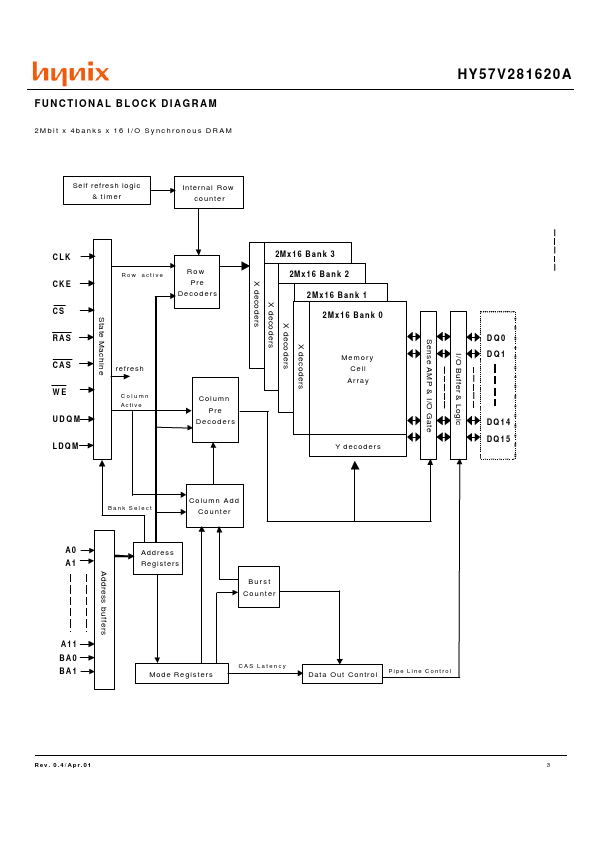
The Hynix HY57V281620A is a 134,217,728bit CMOS Synchronous DRAM, ideally suited for the Mobile applications which require low power consumption and extended temperature range . HY57V281620A is organized as 4banks of 2,097,152x16 H Y 5 7 V 2 8 1 6 2 0 A i s o f f e r i n g f u l l y s y n c h r o n o u s o p e r a t i o n r e f e r e n c e d t o a p o s i t i v e e d g e o f t h e c l o c k . A l l i n p u t s a n d o u t p u t s a r e s y n ch r o nized with the rising edge of the clock input. The data paths are internally pipelined to achieve very high bandwidth. All input and output voltage levels are patible with...