ICSSSTUA32S869B
ICSSSTUA32S869B is 14-Bit Configurable Registered Buffer manufactured by ICS.
..
Integrated Circuit Systems, Inc.
ICSSSTUA32S869B Advance Information
14-Bit Configurable Registered Buffer for DDR2
Remended Application:
- DDR2 Memory Modules
- Provides plete DDR DIMM solution with ICS97U877
- Ideal for DDR2 400, 533 and 667 Product Features
:
- 14-bit 1:2 registered buffer with parity check functionality
- Supports SSTL_18 JEDEC specification on data inputs and outputs
- 50% more dynamic driver strength than standard SSTU32864
- Supports LVCMOS switching levels on C1 and RESET# inputs
- Low voltage operation VDD = 1.7V to 1.9V
- Available in 150 BGA package
- Green packages available
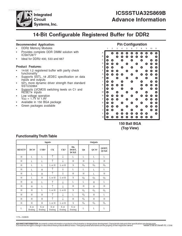
Pin Configuration
1 A B C D E F G H J K L M N P R T U V W 2 3 4 5 6 7 8 9 10 11
150 Ball BGA (Top View) Functionality Truth Table
Inputs RESET# H H H H H H H H H H H H L DCS# L L L L L L H H H H H H X or floating CSR# L L L H H H L L L H H H X or floating CK CK# Dn, DODT, DCKE L H X L H X L H X L H X X or floating Qn L H Q0 L H Q0 L H Q0 Q0 Q0 Q0 L Outputs QCS# L L Q0 L L Q0 H H Q0 H H Q0 L QODT, QCKE L H Q0 L H Q0 L H Q0 L H Q0 L
↑ ↑
L or H
↓ ↓
L or H
↑ ↑
L or H
↓ ↓
L or H
↑ ↑
L or...