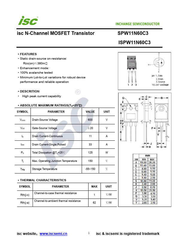
Full PDF Text Transcription for SPW11N60C3 (Reference)
Note: Below is a high-fidelity text extraction (approx. 800 characters) for
SPW11N60C3. For precise diagrams, and layout, please refer to the original PDF.
n-source on-resistance: RDS(on)≤380mΩ ·Enhancement mode: ·100% avalanche tested ·Minimum Lot-to-Lot variations for robust device performance and reliable operation ·DESCRITION · High peak current capability ·ABSOLUTE MAXIMUM RATINGS(Ta=25℃) SYMBOL PARAMETER VALUE VDSS Drain-Source Voltage 600 VGS Gate-Source Voltage ±20 ID Drain Current-Continuous 11 IDM Drain Current-Single Pulsed 33 PD Total Dissipation @TC=25℃ 125 Tj Max.