SPW11N60CFD Overview
Key Specifications
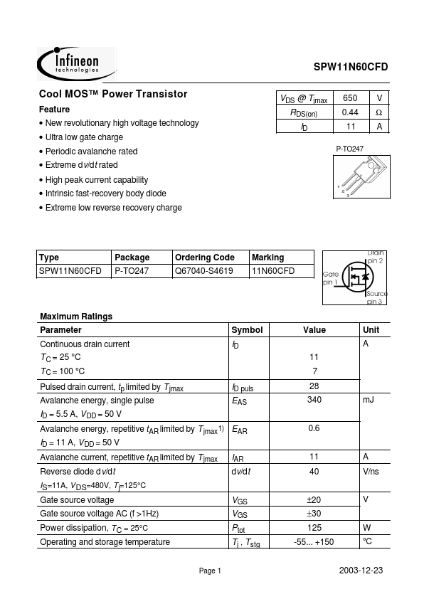
Package: TO-247-3
Pins: 3
Max Operating Temp: 150 °C
Min Operating Temp: -55 °C
Key Features
- New revolutionary high voltage technology
- Ultra low gate charge
- Periodic avalanche rated
- Extreme d v/dt rated
- High peak current capability