DE275-201N25A Description
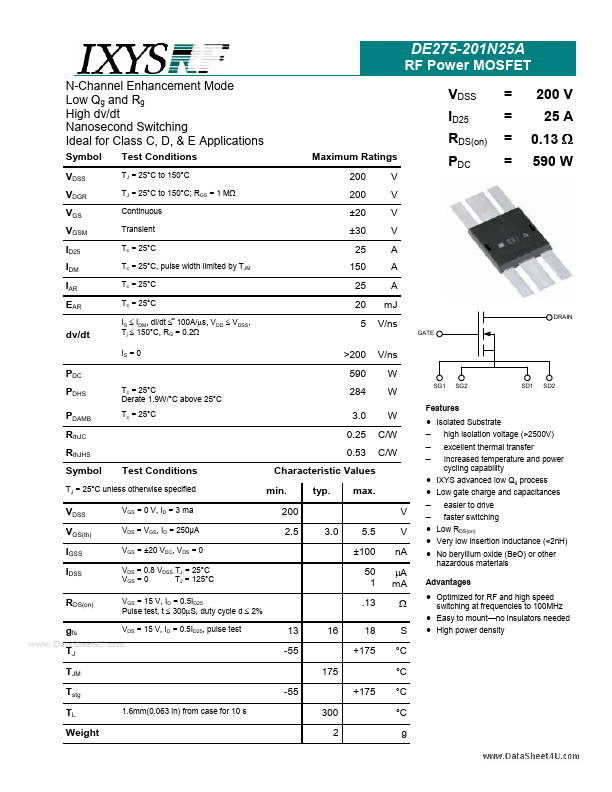
DE275-201N25A RF Power MOSFET N-Channel Enhancement Mode Low Qg and Rg High dv/dt Nanosecond Switching Ideal for Class C, D, & E Applications Symbol VDSS VDGR VGS VGSM ID25 IDM IAR EAR dv/dt Test Conditions TJ = 25°C to 150°C TJ = 25°C to 150°C;.
DE275-201N25A Key Features
- Isolated Substrate
- high isolation voltage (>2500V)
- excellent thermal transfer
- Increased temperature and power
- cycling capability IXYS advanced low Qg process Low gate charge and capacitances easier to drive faster switching Low RD
- Optimized for RF and high speed
- Easy to mount-no insulators needed
- High power density


