IXFC13N50
IXFC13N50 is HiPerFET MOSFET ISOPLUS220 manufactured by IXYS.
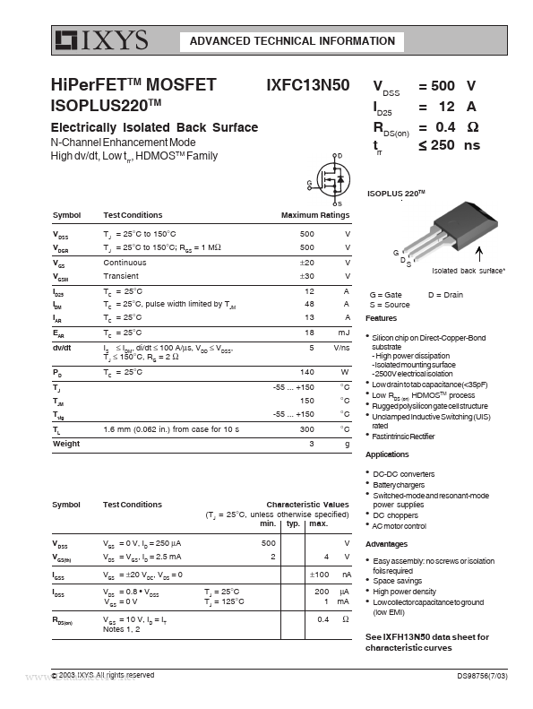
ADVANCED TECHNICAL INFORMATION
HiPerFETTM MOSFET
ISOPLUS220TM
Electrically Isolated Back Surface
N-Channel Enhancement Mode High dv/dt, Low trr, HDMOSTM Family
VDSS ID25 RDS(on) trr
= 500 = 12 = 0.4 ≤ 250
V A Ω ns
ISOPLUS 220TM Symbol VDSS VDGR VGS VGSM ID25 IDM IAR EAR dv/dt PD TJ TJM Tstg TL Weight 1.6 mm (0.062 in.) from case for 10 s Test Conditions TJ = 25°C to 150°C TJ = 25°C to 150°C; RGS = 1 MΩ Continuous Transient TC = 25°C TC = 25°C, pulse width limited by TJM TC = 25°C TC = 25°C IS ≤ IDM, di/dt ≤ 100 A/µs, VDD ≤ VDSS, TJ ≤ 150°C, RG = 2 Ω TC = 25°C Maximum Ratings 500 500 ± 20 ± 30 12 48 13 18 5 140 -55 ... +150 150 -55 ... +150 300 3 V V V V A A A mJ V/ns W °C...