QS532805A
QS532805A is GUARANTEED LOW SKEW 3.3V CMOS CLOCK DRIVER/BUFFER manufactured by Integrated Device Technology.
- Part of the QS532805 comparator family.
- Part of the QS532805 comparator family.
QS532805/A/B GUARANTEED LOW SKEW 3.3V CMOS CLOCK DRIVER/BUFFER
INDUSTRIAL TEMPERATURE RANGE
GUARANTEED LOW SKEW 3.3V CMOS CLOCK DRIVER/BUFFER
Features
:
- -
- -
- -
- - JEDEC patible LVTTL level inputs and outputs 10 output, low skew clock signal buffer Monitor output Clock inputs are 5V tolerant Pinout and function patible with QS5805T 25Ω on-chip resistors for low noise Input hysteresis for better noise margin Guaranteed low skew:
- 0.7ns output skew
- 0.7ns pulse skew
- 1ns part-to-part skew Std., A, and B speed grades (B speed in QSOP package only) Available in QSOP and SOIC packages
QS532805/A/B
DESCRIPTION
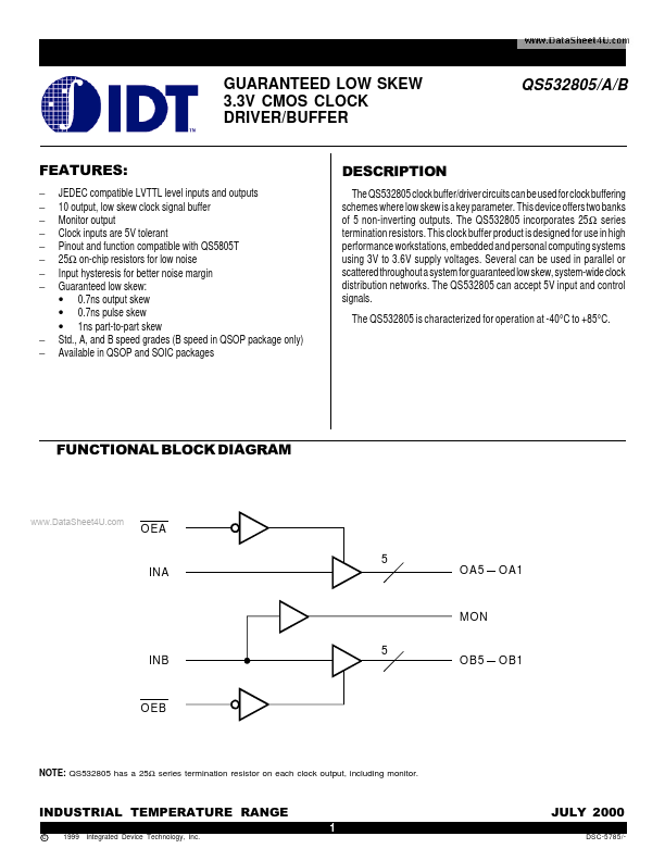
The QS532805 clock buffer/driver circuits can be used for clock buffering schemes where low skew is a key parameter. This device offers two banks of 5 non-inverting outputs. The QS532805 incorporates 25 Ω series termination resistors. This clock buffer product is designed for use in high performance workstations, embedded and personal puting systems using 3V to 3.6V supply voltages. Several can be used in parallel or scattered throughout a system for guaranteed low skew, system-wide clock distribution networks. The QS532805 can accept 5V input and control signals. The QS532805 is characterized for operation at -40°C to +85°C.
- -
FUNCTIONAL BLOCK DIAGRAM
..
OEA 5 INA OA5 OA1
MON 5 INB OB5 OB1
NOTE: QS532805 has a 25Ω series termination resistor on each clock output, including monitor.
INDUSTRIAL TEMPERATURE RANGE
1 c 1999 Integrated Device Technology, Inc.
JULY 2000
DSC-5785/-
QS532805/A/B GUARANTEED LOW SKEW 3.3V CMOS CLOCK DRIVER/BUFFER
INDUSTRIAL TEMPERATURE RANGE
PIN CONFIGURATION
V C CA OA 1 OA 2 OA 3 GND A OA 4 OA 5 GNDQ OE A IN A 1 2 3 4 5 6 7 8 9 10 20 19 18 17 SO 20-2 16 SO 20-8 15 14 13 12 11 V C CB OB1 OB2 OB3 G ND B OB4 OB5 MON OEB IN...


