QS532806A
QS532806A is Guaranteed Low Skew 3.3V CMOS Clock Driver/buffer manufactured by Integrated Device Technology.
- Part of the QS532806 comparator family.
- Part of the QS532806 comparator family.
QS532806/A GUARANTEED LOW SKEW 3.3V CMOS CLOCK DRIVER/BUFFER
INDUSTRIAL TEMPERATURE RANGE
GUARANTEED LOW SKEW 3.3V CMOS CLOCK DRIVER/BUFFER
Features
:
- -
- -
- -
- - JEDEC patible LVTTL level 10 low skew clock outputs Monitor output Clock inputs are 5V tolerant Pinout and function patible with QS5806 25Ω on-chip resistors for low noise Input hysteresis for better noise margin Guaranteed low skew:
- 0.7ns output skew (same bank)
- 0.9ns output skew (different bank)
- 1ns part-to-part skew Std. and A speed grades Available in QSOP and SOIC packages
QS532806/A
DESCRIPTION
The QS532806 clock driver/buffer circuit can be used for clock buffering schemes where low skew is a key parameter. The QS532806 offers two banks of five inverting outputs. Designed in IDT's proprietary CMOS process, these devices provide low propagation delay buffering with onchip skew of 0.7ns for same-transition, same-bank signals. The QS532806 has on-chip series termination resistors for lower noise clock signals. The series resistor versions are remended for driving unterminated lines with capacitive loading and other noise sensitive clock distribution circuits. These clock buffer products are designed for use in high-performance workstations, embedded and personal puting systems. Several devices can be used in parallel or scattered throughout a system for guaranteed low skew, system-wide clock distribution networks.
- -
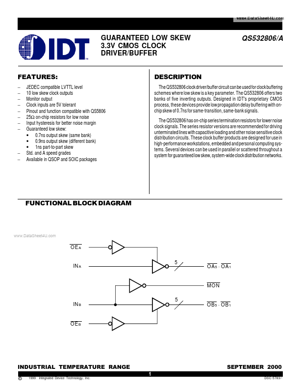
FUNCTIONAL BLOCK DIAGRAM
..
OEA 5
IN A
O A5
- O A1
MO N 5 O B5
- O B1
IN B
INDUSTRIAL TEMPERATURE RANGE
1 c 1999 Integrated Device Technology, Inc.
SEPTEMBER 2000
DSC-5783/-
QS532806/A GUARANTEED LOW SKEW 3.3V CMOS CLOCK...