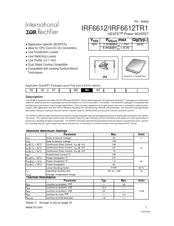
IRF6612 Overview
Description
The IRF6612 combines the latest HEXFET® Power MOSFET Silicon technology with the advanced DirectFET TM packaging to achieve the lowest on-state resistance in a package that has the footprint of a SO-8 and only 0.7 mm profile. The DirectFET package is compatible with existing layout geometries used in power applications, PCB assembly equipment and vapor phase, infra-red or convection soldering techniques, when application note AN-1035 is followed regarding the manufacturing methods and processes.


