2SD1760 Overview
Key Specifications
Package: TO-252-3
Mount Type: Surface Mount
Pins: 3
Max Frequency: 90 MHz
Key Features
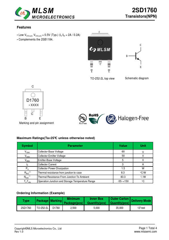
- Low VCE(sat). VCE(sat) = 0.5V (Typ.) (IC/IB = 2A / 0.2A)
- XXXX C B E Marking and pin assignment TO-252-2L top view
| Part | 2SD1760 |
|---|---|
| Description | NPN Transistors |
| Category | Transistor |
| Manufacturer | MLS Microelectronics |
| Size | 747.93 KB |
Package: TO-252-3
Mount Type: Surface Mount
Pins: 3
Max Frequency: 90 MHz
| Seller | Inventory | Price Breaks | Buy |
|---|---|---|---|
| DigiKey | 0 | 1+ : 1.18 USD | View Offer |
| DigiKey | 0 | 1+ : 1.18 USD | View Offer |
| Part Number | Manufacturer | Description |
|---|---|---|
| D1760 | ROHM | 2SD1760 |
| 2SD1760 | Galaxy Microelectronics | NPN Silicon Epitaxial Planar Transistor |
| 2SD1760 | Kexin Semiconductor | NPN Transistors |
| 2SD1760 | Inchange Semiconductor | Silicon NPN Power Transistor |
| 2SD1760 | ROHM | Power Transistor |