MT8332N3
MT8332N3 is N-Channel Enhancement Mode Field Effect Transistor manufactured by MT Semiconductor.
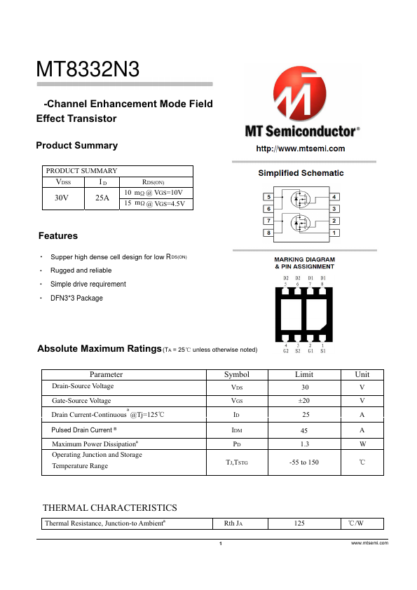
Features
6XSSHUKLJKGHQVHFHOOGHVLJQIRUORZ R'621 5XJJHGDQGUHOLDEOH Simple drive requirement DFN3- 3 Package
Absolute Maximum Ratings(TA = 25 unless otherwise noted)
Parameter
Drain-Source Voltage
Gate-Source Voltage Drain Current-Continuous嘌@Tj=125ć
Pulsed Drain Current B Maximum Power Dissipation嘌 Operating Junction and Storage Temperature Range
Symbol
VDS VGS ID IDM PD
TJ,TSTG
Limit
30 ±20
25 45 1.3
-55 to 150
Unit
V V A A W
ć
THERMAL CHARACTERISTICS
Thermal Resistance, Junction-to Ambient嘌
Rth JA
ć/W
ZZZPWVHPLFRP
ELECTRICAL CHARACTERISTICS (T A=25ć unless otherwise noted)
Parameter
OFF CHARACTERISTICS
Symbol
Condition
Drain-Source Breakdown Voltage Zero Gate Voltage Drain Current Gate-Body Leakage
ON CHARACTERITICS
BVDSS IDSS IGSS
VGS=0V,ID=250 嘕 A VDS=24V,V GS =0V VGS = ±24V,VDS =0V
Gate Threshold Voltage
VGS(th)
V DS=VGS,ID=250 嘕A
Drain-Source On-State Resistance
RDS(ON)
VGS=10V,I D =10A VGS =4.5V,ID...