ME3500-G
ME3500-G is N- & P-Channel 30V (D-S) MOSFET manufactured by Matsuki.
- Part of the ME3500 comparator family.
- Part of the ME3500 comparator family.
DESCRIPTION
The ME3500 is the N- and P-Channel logic enhancement mode power field effect transistors are produced using high cell density , DMOS trench technology. This high density process is especially tailored to minimize on-state resistance. These devices are particularly suited for low voltage application such as cellular phone and notebook puter power management and other battery powered circuits where high-side switching, and low in-line power loss are needed in a very small outline surface mount package.
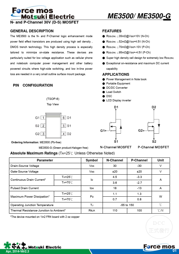
PIN CONFIGURATION
(TSOP-6) Top View
ME3500/ ME3500-G
FEATURES
- RDS(ON) ≦35mΩ@VGS=10V (N-Ch)
- RDS(ON) ≦52mΩ@VGS=4.5V (N-Ch)
- RDS(ON) ≦70mΩ@VGS=-10V (P-Ch)
- RDS(ON) ≦95mΩ@VGS=-4.5V (P-Ch)
- Super high density cell design for extremely low RDS(ON)
- Exceptional on-resistance and maximum DC current capability
APPLICATIONS
- Power Management in Note book
- Portable Equipment
- DC/DC Converter
-...