Datasheet4U Logo Datasheet4U.com

MCM69D536 - 32K x 36 Bit Synchronous Dual I/O / Dual Address SRAM

Datasheet Summary

Description

Pin Locations 65, 63, 61, 59, 57, 55, 169, 167, 145, 143, 68, 70, 72, 74, 76 64, 62, 60, 58, 56, 54, 168, 166, 144, 142, 69, 71, 73, 75, 77 82, 86, 90, 94, 96, 100, 102, 106, 108, 113.

Features

  • common data input and data output buffers and incorporates input and output registers on.
  • board with high speed SRAM. The MCM69D536 allows the user to concurrently perform reads, writes, or pass.
  • through cycles in combination on the two data ports. The two address ports (AX, AY) determine the read or write locations for their respective data ports (DQX, DQY). The synchronous design allows for precise cycle control with the use of an external single clock (K). All signal pins except.

📥 Download Datasheet

Datasheet preview – MCM69D536

Datasheet Details

Part number MCM69D536
Manufacturer Motorola
File Size 212.44 KB
Description 32K x 36 Bit Synchronous Dual I/O / Dual Address SRAM
Datasheet download datasheet MCM69D536 Datasheet
Additional preview pages of the MCM69D536 datasheet.
Other Datasheets by Motorola

Full PDF Text Transcription

Click to expand full text
MOTOROLA SEMICONDUCTOR TECHNICAL DATA Order this document by MCM69D536/D 32K x 36 Bit Synchronous Dual I/O, Dual Address SRAM
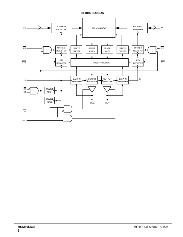
 The MCM69D536 is a 1M–bit static random access memory, organized as 32K words of 36 bits. It features common data input and data output buffers and incorporates input and output registers on–board with high speed SRAM. The MCM69D536 allows the user to concurrently perform reads, writes, or pass–through cycles in combination on the two data ports. The two address ports (AX, AY) determine the read or write locations for their respective data ports (DQX, DQY). The synchronous design allows for precise cycle control with the use of an external single clock (K). All signal pins except output enables (GX, GY) are registered on the rising edge of clock (K).
Published: |