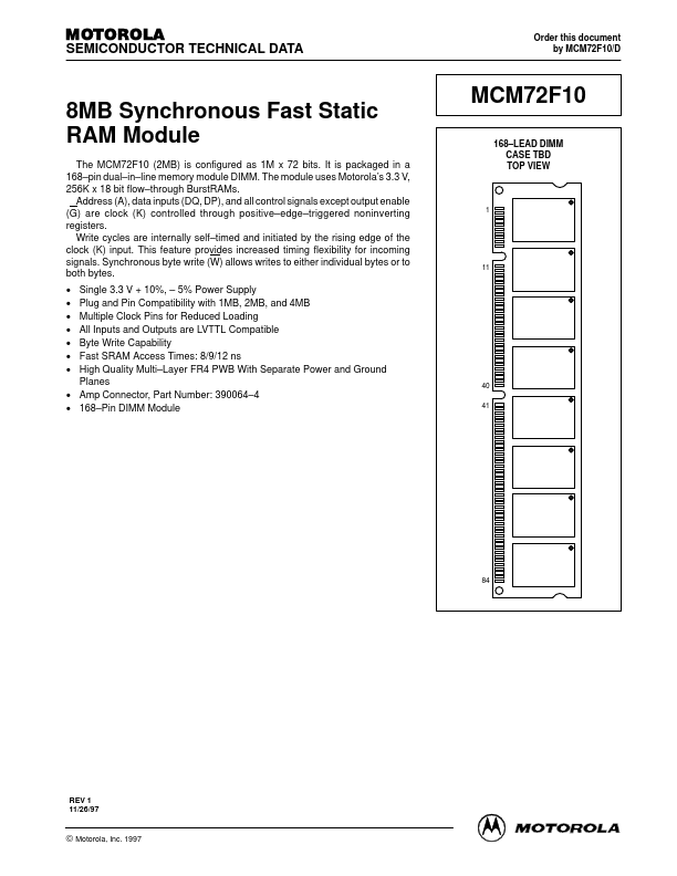
Datasheet4U Logo Datasheet4U.com

MCM72F10 - 8MB Synchronous Fast Static RAM Module

Description

Pin Locations 59, 61, 62, 64, 65, 67, 68, 70, 71, 72, 143, 145, 146, 148, 149, 151, 152, 154, 155 156 15, 31, 44, 86, 92, 105, 121, 134 2, 3, 5, 6, 8, 9, 11, 12, 14, 17, 18, 20, 21, 23, 24, 26, 27, 32, 34, 35, 37, 38, 40, 41, 43, 46, 47, 49, 50, 52, 53, 55, 56, 87, 89, 90, 93, 95, 96, 98, 99, 101,

Features

  • upply Voltage (Operating Voltage Range) Input High Voltage Input Low Voltage.
  • VIL ≥.
  • 2.0 V for t ≤ tKHKH/2. VIH Symbol VDD VIH VIL Min 3.135 1.7.
  • 0.3.
  • Typ 3.3.
  • Max 3.6 VDD + 0.3 0.7 Unit V V V VSS VSS.
  • 1.0 V 20% tKHKH (MIN) Figure 1. Undershoot Voltage DC.

📥 Download Datasheet

Datasheet preview – MCM72F10

Datasheet Details

Part number MCM72F10
Manufacturer Motorola
File Size 138.59 KB
Description 8MB Synchronous Fast Static RAM Module
Datasheet download datasheet MCM72F10 Datasheet
Additional preview pages of the MCM72F10 datasheet.
Other Datasheets by Motorola

Full PDF Text Transcription

Click to expand full text
MOTOROLA SEMICONDUCTOR TECHNICAL DATA Order this document by MCM72F10/D 8MB Synchronous Fast Static RAM Module The MCM72F10 (2MB) is configured as 1M x 72 bits. It is packaged in a 168–pin dual–in–line memory module DIMM. The module uses Motorola’s 3.3 V, 256K x 18 bit flow–through BurstRAMs. Address (A), data inputs (DQ, DP), and all control signals except output enable (G) are clock (K) controlled through positive–edge–triggered noninverting registers. Write cycles are internally self–timed and initiated by the rising edge of the clock (K) input. This feature provides increased timing flexibility for incoming signals. Synchronous byte write (W) allows writes to either individual bytes or to both bytes. • • • • • • • Single 3.
Published: |