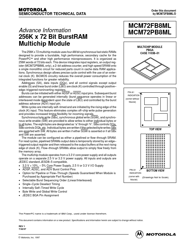
Datasheet4U Logo Datasheet4U.com

MCM72FB8ML - 256K x 72 Bit Burst RAM Multichip Module

General Description

Pin Locations E10 Symbol ADSC Type Input Description Synchronous Address Status Controller: Active low, interrupts any ongoing burst and latches a new external address.

Used to initiate READ, WRITE, or chip deselect cycle.

Key Features

  • br>.
  • Z High.
  • Z High.
  • Z High.
  • Z Write 2, 4 X X X X X X5 READ5 READ READ READ READ READ READ READ READ WRITE WRITE WRITE WRITE WRITE NOTES: 1. X = Don’t Care. 1 = logic high. 0 = logic low. 2. Write is defined as either 1) any SBx and SW low or 2) SGW is low. 3. G is an asynchronous signal and is not sampled by the clock K. G drives the bus immediately (tGLQX) following G going low. 4. On write cycl.

📥 Download Datasheet

Full PDF Text Transcription (Reference)

The following content is an automatically extracted verbatim text from the original manufacturer datasheet and is provided for reference purposes only.

View original datasheet text
MOTOROLA SEMICONDUCTOR TECHNICAL DATA Order this document by MCM72FB8ML/D Advance Information 256K x 72 Bit BurstRAM Multichip Module The 256K x 72 multichip module uses four 4M bit synchronous fast static RAMs designed to provide a burstable, high performance, secondary cache for the PowerPC™ and other high performance microprocessors. It is organized as 256K words of 72 bits each. This device integrates input registers, an output register (MCM72PB8ML only), a 2–bit address counter, and high speed SRAM onto a single monolithic circuit for reduced parts count in cache data RAM applications. Synchronous design allows precise cycle control with the use of an external clock (K). BiCMOS circuitry reduces the overall power consumption of the integrated functions for greater reliability.