UPA1708
Overview
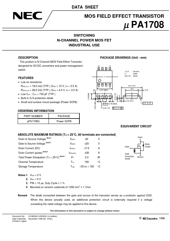
This product is N-Channel MOS Field Effect Transistor designed for DC/DC converters and power management switch. 8 PACKAGE DRAWINGS (Unit : mm) 5 1,2,3 ; Source ; Gate 4 5,6,7,8 ; Drain.
- Low on-resistance RDS(on)1 = 18.0 mΩ (TYP.) (VGS = 10 V, ID = 3.5 A)
- 44 1 5.37 MAX. +0.10 -0.05 4
- 0 ±0.3 4.4 0.8 RDS(on)2 = 28.0 mΩ (TYP.) (VGS = 4.5 V, ID = 3.5 A)
- Low Ciss : Ciss = 730 pF (TYP.)
- Built-in G-S protection diode
- Small and surface mount package (Power SOP8)
- 8 MAX.
- 05 MIN.
- 5 ±0.2 0.10
- 27 0.78 MAX. 0.40 +0.10 -0.05