UPA2753GR
DESCRIPTION
The µPA2753GR is Dual N-Channel MOS Field Effect Transistor designed for DC/DC converters and power management applications of notebook puters.
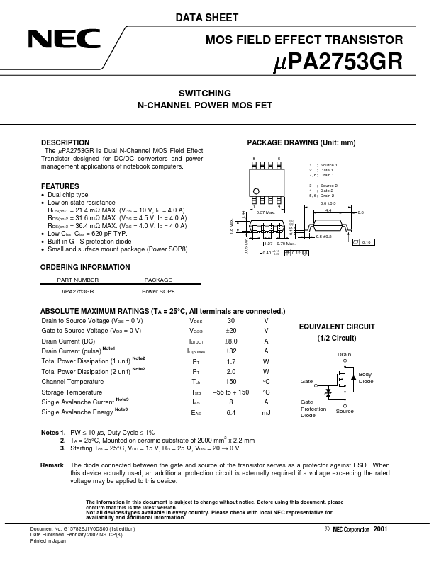
PACKAGE DRAWING (Unit: mm)
8 5 1 ; Source 1 2 ; Gate 1 7, 8 ; Drain 1 3 ; Source 2 4 ; Gate 2 5, 6 ; Drain 2 1 4 5.37 Max.
+0.10
- 0.05
FEATURES
- Dual chip type
- Low on-state resistance RDS(on)1 = 21.4 mΩ MAX. (VGS = 10 V, ID = 4.0 A) RDS(on)2 = 31.6 mΩ MAX. (VGS = 4.5 V, ID = 4.0 A) RDS(on)3 = 36.4 mΩ MAX. (VGS = 4.0 V, ID = 4.0 A)
- Low Ciss: Ciss = 620 p F TYP.
- Built-in G
- S protection diode
- Small and surface mount package (Power SOP8)
6.0 ±0.3 4.4 0.8
1.8 Max.
0.05 Min.
0.5 ±0.2 0.10
1.27 0.40
0.78 Max. 0.12 M
+0.10
- 0.05
ORDERING INFORMATION
PART NUMBER PACKAGE Power SOP8
µPA2753GR
ABSOLUTE MAXIMUM RATINGS (TA = 25°C, All terminals are connected.)
Drain to Source Voltage (VGS = 0 V) Gate to Source Voltage (VDS = 0 V) Drain Current (DC) Drain Current (pulse)
Note1 Note2 Note2
VDSS VGSS ID(DC)...