Description
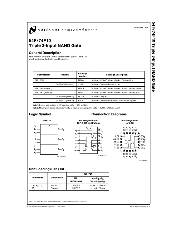
This device contains three independent gates each of which performs the logic NAND function mercial 74F10PC Military Package Number N14A Package Description 14-Lead (0 300 Wide) Molded Dual-In-Line 14-Lead Ceramic Dual-In-Line 14-Lead (0 150 Wide) Molded Small Outline JEDEC 14-Lead (0 300 Wide) Molded Small Outline EIAJ 14-Lead Cerpack 20-Lead Ceramic Leadless Chip Carrier Type C 54F10DM (Note 2) 74F10SC (Note 1) 74F10SJ (Note 1) 54F10FM (Note 2) 54F10LM (Note 2) J14A M14A M14D W14B E20A Note 1 Devices also available in 13 reel Use suffix e SCX and SJX Note 2 Military grade device with environmental and burn-in processing Use suffix e DMQB FMQB and LMQB Logic Symbol IEEE IEC Connection Diagrams Pin Assignment for DIP SOIC and Flatpak Pin Assignment for LCC TL F 9458-3 TL F 9458 - 2 TL F 9458 - 1 Unit Loading Fan Out 54F 74F Pin Names Description UL HIGH LOW 10 10 50 33 3 Input IIH IIL Output IOH IOL 20 mA b0 6 mA b 1 mA 20 mA An Bn Cn On Inputs Outputs FAST and TRI-STATE are registered trademarks of National Semiconductor Corporation C1995 National Semiconductor Corporation TL F 9458 RRD-B30M75 Printed in U S A If Military Aerospace specified devices are required please contact the National Semiconductor Sales Office Distributors for availability and specifications Storage Temperature Ambient Temperature under Bias Junction Temperature under Bias Plastic VCC Pin Potential to Ground Pin b 65 C to a 150 b 55 C to a 125 b 55 C to a 175 b 55 C to a 150 Remended Operating Conditions Free Air Ambient Temperature Military mercial Supply Voltage Military mercial b 55 C to a 125 C 0 C to a 70 C a 4 5V to a 5 5V a 4 5V to a 5 5V C C C C b 0 5V to a 7 0V b 0 5V to a 7 0V Input Voltage (Note 2) b 30 mA to a 5 0 mA Input Current (Note 2) Voltage Applied to Output in HIGH State (with VCC e 0V) b 0 5V to VCC Standard Output b 0 5V to a 5 5V TRI-STATE Output Current Applied to Output in LOW State (Max) twice the rated IOL (mA) Note 1 DC Symbol VIH VIL VCD VOH Parameter Min Input HIGH Voltage Input LOW Voltage Input Clamp Diode Voltage Output HIGH Voltage Output LOW Voltage Input HIGH Current Input HIGH Current Breakdown Test Output HIGH Leakage Current Input Leakage Test Output Leakage Circuit Current Input LOW Current Output Short-Circuit Current Power Supply Current Power Supply Current b 60 54F 74F Typ Max Units V 08 b1 2 VCC Conditions Recognized as a HIGH Signal Recognized as a LOW Signal 20 V V V Min Min IIN e b18 mA IOH e b1 mA IOH e b1 mA IOH e b1 mA IOL e 20 mA IOL e 20 mA VIN e 2 7V VIN e 7 0V VOUT e VCC IID e 1 9 mA All other pins grounded VIOD e 150 mV All other pins grounded VIN e 0 5V VOUT e 0V VO e HIGH VO e LOW 54F 10% VCC 74F 10% VCC 74F 5% VCC 54F 10% VCC 74F 10% VCC 54F 74F 54F 74F 54F 74F 74F 74F 25 25 27 05 05 20 0 50 100 70 250 50 4 75 3 75 b0 6 b 150 VOL IIH IBVI ICEX VID IOD IIL IOS ICCH ICCL V mA mA mA V mA mA mA mA mA Min Max Max Max 00 00 Max Max Max Max 14 51 21 77 2 AC 74F Symbol Parameter Min tPLH tPHL Propagation Delay An Bn Cn to On 24 15 TA e a 25 C VCC e a 5 0V CL e 50 pF Typ 37 32 Max 50 43 54F TA VCC e Mil CL e 50 pF Min 20 15 Max 70 65 74F TA VCC e CL e 50 pF Min 24 15 Max 60 53 ns Units.