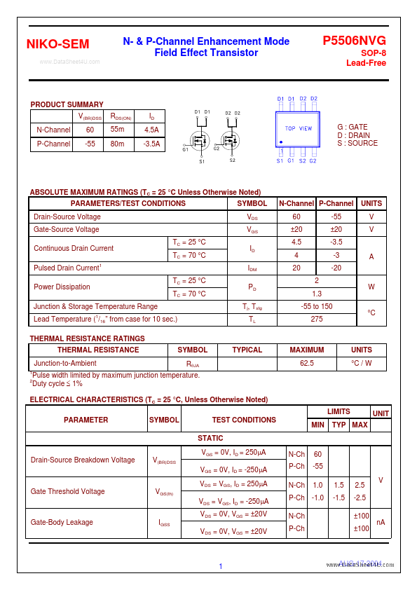
P5506NVG Overview
| Part | P5506NVG |
|---|---|
| Description | N- & P-Channel Enhancement Mode Field Effect Transistor |
| Category | Transistor |
| Manufacturer | Niko |
| Size | 555.79 KB |
| Seller | Inventory | Price Breaks | Buy |
|---|---|---|---|
| ICPartonline | 32072 | 1+ : 28 USD 10+ : 26.6 USD 100+ : 25.2 USD 1000+ : 23.8 USD |
View Offer |
| Antdic Electronics | 19379 | 1+ : 7 USD 10+ : 6.65 USD 100+ : 6.3 USD 1000+ : 5.6 USD |
View Offer |
| Part Number | Manufacturer | Description |
|---|---|---|
| P5506NVG | UNIKC | N&P-Channel MOSFET |
| P5506BDG | UNIKC | N-Channel MOSFET |
| P5506HPG | NIKO-SEM | Dual N-Channel MOSFET |
| P5506BDA | Inchange Semiconductor | N-Channel MOSFET |
| P5506BVG | UNIKC | N-Channel MOSFET |